
 |
|
Biography
Mahdi Pourfath was born in Tehran, Iran, in 1978. He studied electrical engineering at the Sharif University of Technology, where he received the MSc degree in 2002. He joined the Institute for Microelectronics in October 2003, where he received his doctoral degree in technical sciences in July 2007 and is currently employed as a project assistant.
Modeling Nanoscaled Transistors Based on Single Layer MoS2
Since the successful experimental isolation of graphene in 2004, ultra-thin two-dimensional structures are being widely studied as potential building blocks for future electronic devices. Graphene exhibits some remarkable electronic properties, however, the absence of a bandgap has so far precluded its exploitation in electronic applications. Several strategies have been proposed to open a gap, but a bandgap larger than 400meV remains a challenge. Other two-dimensional materials, however, show an intrinsic non-zero bandgap. Due to a two-dimensional structure similar to graphene, transition metal dichalcogenides have recently attracted the attention of the scientific community. These materials form layered structures, where layers are held together by Van der Waals interactions. Because of the weak inter-layer van der Waals bonds in their layered structure, single layers and few-layers of these materials can be obtained by mechanical or chemical exfoliation techniques. Out of the transition metal dichalcogenide family, MoS2 is of particular interest. A single MoS2 layer is composed of one atomic layer of molybdenum sandwiched between two atomic layers of sulfur. Recently, field effect transistors based on single-layer MoS2 with an on/off current ratio of eight orders of magnitude and a sub-threshold swing of ~70mV/decade have been reported. The near ideal sub-threshold swing is due to the strong suppression of short channel effects in low-dimensional materials and excellent electrostatic control of the gate over the channel. We employed ab-initio simulation to evaluate the electronic bandstructure of this material and its dependence on strain (see Fig. 1). Thereafter, we solved the linearized Boltzmann equation to obtain low-field mobility. Various scattering mechanisms due to scattering sources, such as intra-valley and inter-valley acoustic phonons, optical and polar optical phonons, remote phonons, and charged impurities, have been considered. Furthermore, the dynamic screening of remote phonon modes in the dielectric, and static screening of charged impurities are included. We studied the dependences of mobility on strain and also on the dielectric material. To study high field effects and also device characteristics, the non-equilibrium Green's function method has been utilized. This approach allows an accurate description of quantum mechanical phenomena and scattering mechanisms in nanoscaled transistors. With the aid of the developed models one can optimize the performance of MoS2 based transistors.
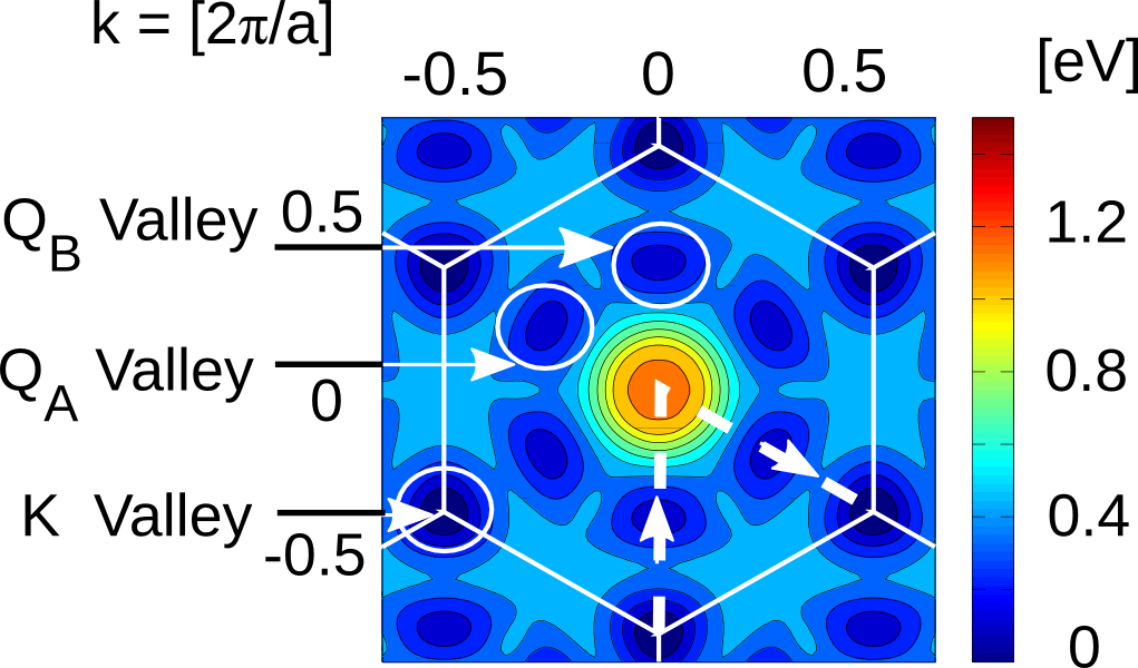
Fig. 1: Equi-energy contours in the first Brillouin zone for unstrained single layer MoS2.