 |
|
Biography
Marco Rovitto was born in Milan, Italy, in 1985. He studied material science at the Università degli Studi di Milano-Bicocca, where he received the bachelor's degree in 2010 and the master's degree in 2013. He joined the Institute for Microelectronics in January 2014, where he is currently working on his doctoral degree. His scientific interests include electromigration, interconnects, and process simulations.
Electromigration Reliability in Open TSVs
Recently, Through Silicon Vias (TSVs) have attracted much attention in three-dimensional (3D) integration technology due to their function as vertical connections of the stacked semiconductor dies. Due to the high mechanical stresses generated around the TSV as a result of the mismatched thermal expansion coefficients of the metal core and the substrate, a new concept for wafer-to-wafer integration based on open TSV technology has been introduced. By introducing the unfilled metal TSV design, the thermo-mechanical issues induced by the material properties are reduced. Although open TSVs have distinctive benefits, the understanding of the reliability issues that can occur in these interconnect structures is now a necessity. TSV reliability issues affect the reliability of the whole interconnect structure and the 3D integrated circuit. A key aspect for reliability assessment of TSVs is ElectroMigration (EM). EM refers to the process of mass transport due to current flow in a metal line, and is the most important metallization wear-out failure mechanism in interconnects. The EM wear-out mechanism is normally due to the formation of a void that eventually grows, causing a chip failure. In 3D open TSV technology, the severe dimension mismatches between landing pads, TSV sidewall and metal wires can lead to a nucleation of a small void triggering a failure mechanism. Consequently, the prediction of the void nucleation time becomes decisive for a precise EM lifetime estimation of a given interconnect. Mathematical modeling can significantly contribute to the comprehension of EM failure mechanisms. Traditionally, a simple mathematical model known as Black’s equation has been used from the early times of EM investigations for the estimation of the interconnect time to failure.
Due to the complexity of the physical phenomenon, 3D TCAD simulation based on a multiphysics EM model has been utilized to identify the locations with the highest probability of void nucleation in the open TSV structure shown in Fig. 1. The stress evolution which leads to the void nucleation in the TSV is simulated by using the finite element method (Fig. 2). The EM time to failure is defined as the time needed to reach the threshold stress at the sites of the void nucleation. Simulations are able to study the EM failure development under the influence of different operating conditions, geometrical features and material properties. The EM lifetime distribution of different interconnects can be predicted and the degradation processes due to reliability issues in the open TSV technologies can be overcome.
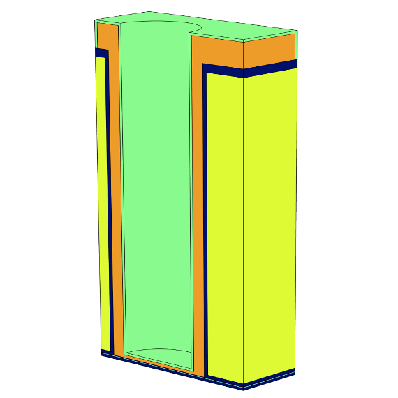
Fig. 1: Profile view of an open TSV structure.
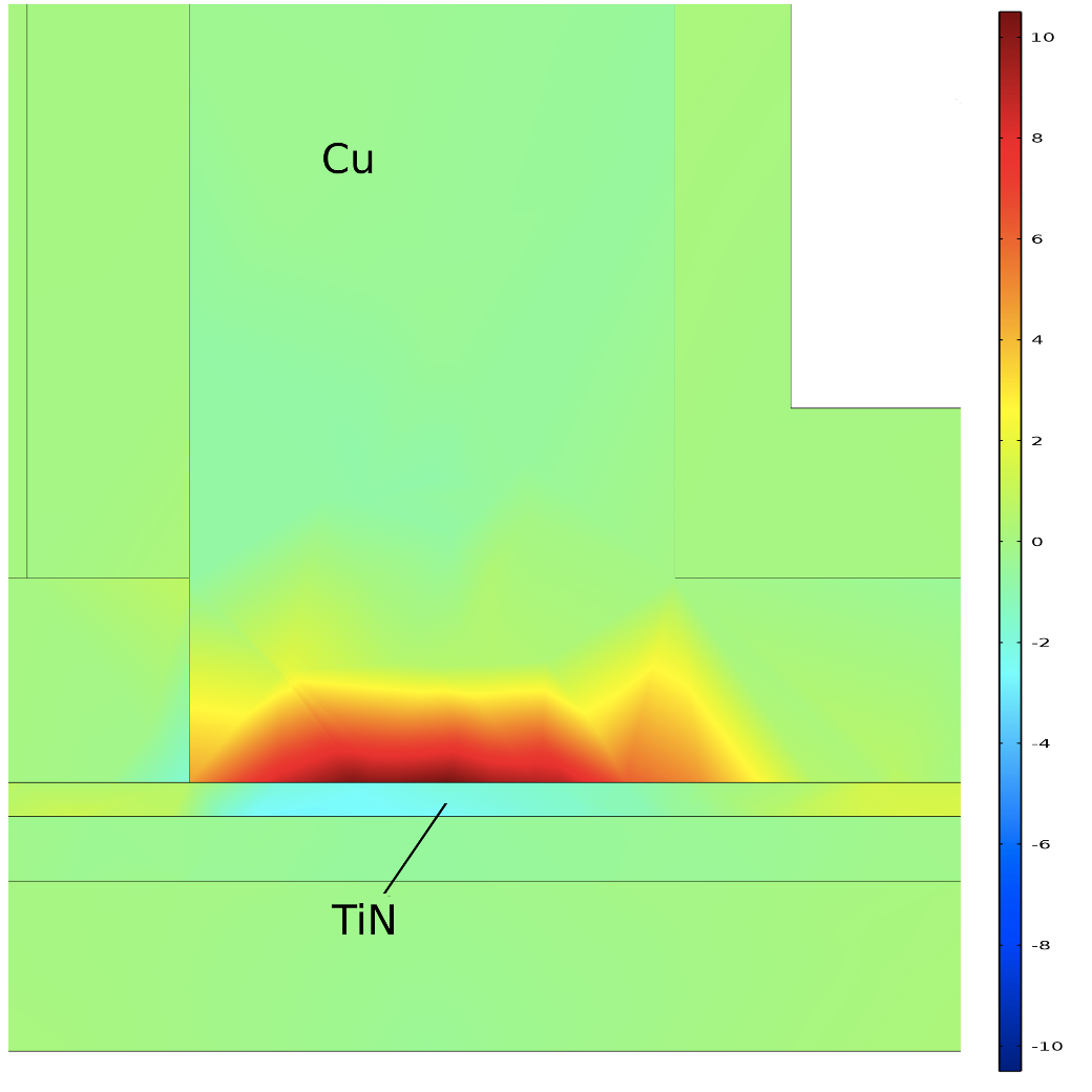
Fig. 2: Stress in the cross section view of the TSV bottom (MPa). The Cu/TiN interface is recognized to be the site of void nucleation in the structure.