 |
|
Biography
Gerhard Rzepa, born in 1985 in Austria, studied at the Technische Universität Wien where he received the BSc degree in electrical engineering and the Diplomingenieur degree in microelectronics in 2010 and 2013, respectively. He joined the Institute for Microelectronics in December 2013, where he is working on his doctoral degree. His current research topic is the microscopic modeling of oxide defects.
Microscopic Oxide Defects Causing BTI, RTN, and SILC on High-K FinFETs
Microscopic modeling of oxide defects in the framework of Nonradiative Multi-Phonon (NMP) theory can explain various reliability issues of MOSFETs, starting from the recoverable component of Bias Temperature Instability (BTI) up to Random Telegraph Noise (RTN). The threshold voltage shift of MOS transistors simulated with the recently proposed four-state NMP model is in perfect agreement with measurement results for various stress conditions including AC signals on large as well as small-area devices. In particular, a stress setup which employs a short pulse into accumulation allows for the distinguishing of contributions of oxide defects from degradation due to interface defects. Encouraged by this successful verification, we have studied single defects in detail. Even though the actual structure of oxide defects is still a subject of debate, their behavior is thoroughly investigated using time-dependent defect spectroscopy, Stress-Induced Leakage Current (SILC) and RTN analysis.
Modeling oxide defects within the NMP theory is in principle straightforward, though its complexity increases greatly when all aspects of MOSFET structures are included. Not only the distribution of carrier energies have to be taken into account correctly, also the tunneling through Fin structures with high-k oxide layers has to be modeled carefully, as it determines the interplay of carrier exchange of the gate and the channel. In order to study reliability issues of high-k FinFET structures, we have extracted the corresponding model parameters based on degradation measurements. The resulting microscopic defects have been investigated in order to understand the degradation mechanisms. This study is shown in Fig. 1 for an exemplary oxide defect. For low stress voltage (top) the trap level is below the Fermi level of both the gate and the channel. The defect is neutral and inactive accordingly. For moderate stress voltage (middle) the capture and emission time constants are on the same order of magnitude, hence RTN can be observed. For large stress voltage (bottom), hole capture from the channel and hole emission to the gate increase significantly and, thereby, the defect contributes to SILC. Furthermore, the capture process is much faster compared to emission which results in an effective positive charge shift, causing a threshold voltage shift as it can be observed in BTI experiments. The fact that the four-state NMP model can describe these reliability issues inherently further supports the validity of the NMP theory for the description of charge exchange of oxide defects.
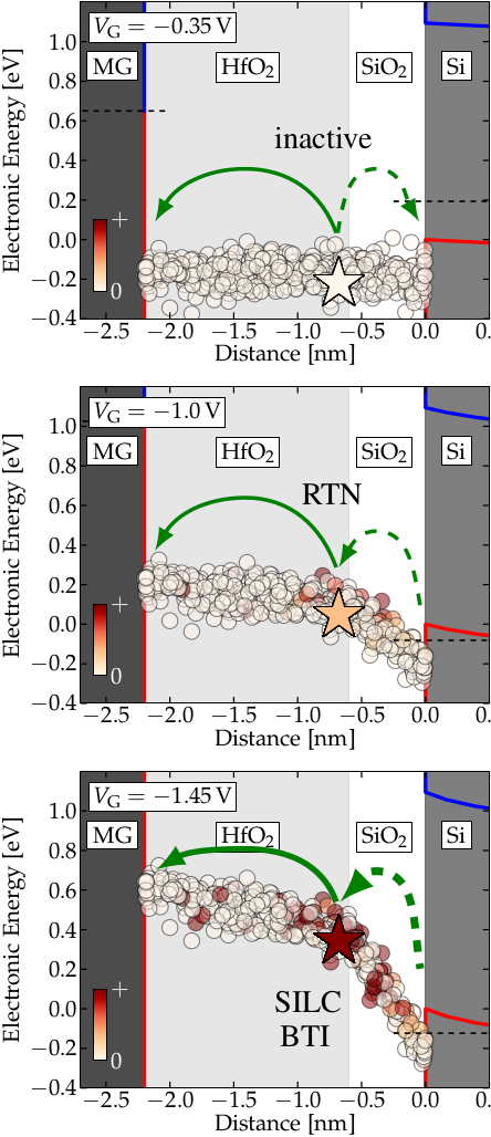
Fig. 1: The interaction of an exemplary oxide defect (star) with the metal gate (MG) and the channel (Si) of an pMOS FinFET. Depending on the stress voltage Vg this defect is either neutral and inactive (top), contributes to RTN (middle), or causes SILC and BTI (bottom).