 |
|
Biography
Prateek Sharma was born in Kota (Rajasthan), India. He recieved degree of Master of Science in electrical engineer from Linköping University, Sweden in 2012, where he was also invovled in smart dust and body area networks research projects. He joined the Institute for Microelectronics in March 2013 where he is working on the realiability systems in microelectronics.
Predictive and Efficient Modeling of HCD in LDMOS transistors
A physical Hot-Carrier Degradation (HCD) model should consider all superpositions of the two competing mechanisms of Si-H bond dissociation, namely, the single- and multiple-carrier processes (driven by hot and cold carriers, respectively). For this purpose, one needs to address carrier transport and evaluate the carrier energy Distribution Function (DF). This DF is obtained, ideally, via solution of the full-band-structure Boltzmann Transport Equation (BTE) which is a very complicated task in power devices because of their complex structures, large dimensions and high operating voltages. As a result, derivation of a predictive HCD model, which can properly capture carrier transport, appears to be difficult. However, simplified approaches to the solution of the BTE, such as Drift-Diffusion (DD) and energy transport schemes, appear to be attractive. These models attempt to mimic the carrier energy distribution function by an analytic expression which is linked to the electric field and the density of carriers found using the DD approach. Although such models are capable of representing the carrier DF with reasonable accuracy, they often fail to properly describe HCD. This is because even small discrepancies in the DF can translate to substantial errors in calculated changes of the device characteristics.
As a reference, we first calculate the DF using our deterministic BTE solver ViennaSHE for nLDMOS and pLDMOS transistors. Then we try to model these DFs using an analytic expression based on the DD scheme. The DFs obtained from both variants are shown in Fig. 1 for the nLDMOS device. Our expression for the DF considers the contribution of both the hot and equilibrium carriers and thus corresponds well to our HCD model. The parameters of the analytical DF are found using the integral equation set comprising the carrier density, carrier temperature and DF normalization. The carrier temperatures are estimated in a post-processing step by the homogeneous energy balance equation using the electric field as well as the carrier mobilities obtained from the DD simulations. The DFs are used as input for our physical HCD model to calculate the acceleration integrals and interface state density profiles. These interface state densities are used by our device simulator MiniMOS-NT to determine the device degradation characteristics. The degradation in saturation drain currents obtained from both versions of the model are in good agreement with the experiment (see Fig. 2). We follow a similar procedure for the pLDMOS transistor, and the simulated saturation drain currents are compared with the experimental data in Fig. 3. For both kinds of devices, the DD- and SHE-based models give similar results and agree well with the experiments suggesting that the efficient DD-based model is well suited for describing HCD in LDMOS devices.
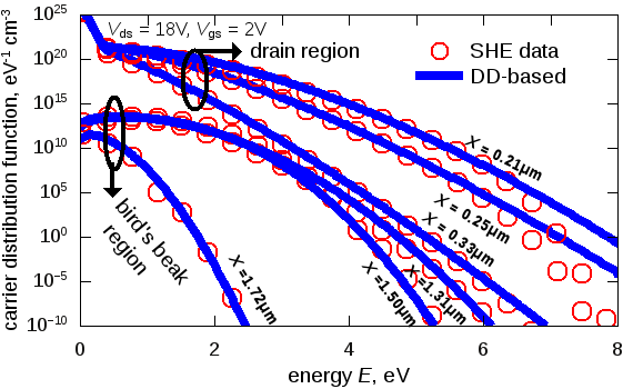
Fig. 1: Comparison of DFs from the DD-based model with those obtained from ViennaSHE for stress voltages: Vds = 18V, Vgs= 2V, calculated for different positions near the drain and bird's beak region in nLDMOS transistors.
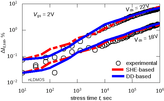
Fig. 2: The change in the saturation drain currents obtained from experiments and simulations using the SHE- and DD-based models for stress voltages Vgs = 2V and Vds = 18V, 22V and stress times up to 1Ms for nLDMOS transistors.
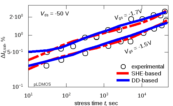
Fig. 3: The change in the saturation and linear drain currents obtained from experiments and simulations using the SHE- and DD-based models for stress voltages Vds = -50V, Vgs = -1.7V and -1.5V and stress times up to 1Ms for pLDMOS transistors.