 |
|
Biography
Oskar Baumgartner was born in Krems an der Donau, Austria, in 1982. He studied electrical engineering at the Technische Universität Wien, where he received the degree of Diplomingenieur in January 2007. He joined the Institute for Microelectronics in February 2007, where he is currently working on his doctoral degree. His scientific interests include the modeling and simulation of quantum transport in optical and nanoelectronic devices.
Investigation of Quantum Transport in Nanoscaled GaN HEMTs
Gallium nitride (GaN) based High-Electron Mobility Transistors (HEMTs) have garnered increasing interest in recent years as viable candidates for high power and high frequency applications. They offer high breakdown voltages due to the wide bandgap, and the strain-induced piezoelectric charge leads to high carrier sheet densities at the hetero interfaces. The high electron mobility allows for high-frequency applications of these devices. More recently, HEMT gate lengths have reached the nano-scale in order to dramatically increase cutoff and maximum oscillation frequency.
We investigated the quantum transport properties of nanoscaled high-frequency GaN HEMTs. For that purpose, a simulation model for quantum transport in nanodevices on unstructured grids in arbitrary dimension and for arbitrary crystal directions has been developed. We model a 2D/3D real-space Schrödinger system with open boundary con:qditions resulting in a consistent treatment of quantization and transport effects. The model has been implemented as part of the Vienna-Schrödinger-Poisson (VSP) quantum electronic simulation and modeling framework. The transport formalism is based on the Quantum-Transmitting Boundary Method (QTBM). A new approach to reduce computational effort has been realized. The model has been used to consistently treat quantization and transport effects in deeply scaled asymmetric GaN HEMTs. We were able to calculate the self-consistent electron concentration, conduction bandedges and ballistic current through the device. Fig. 1 and Fig. 2 show the effects of strain relaxation at the hetero interfaces on the potential and carrier concentration. Due to a larger interface charge in the fully strained device, stronger confinement is achieved. In the relaxed device, on the other hand, a part of the current is flowing through the back barrier region.
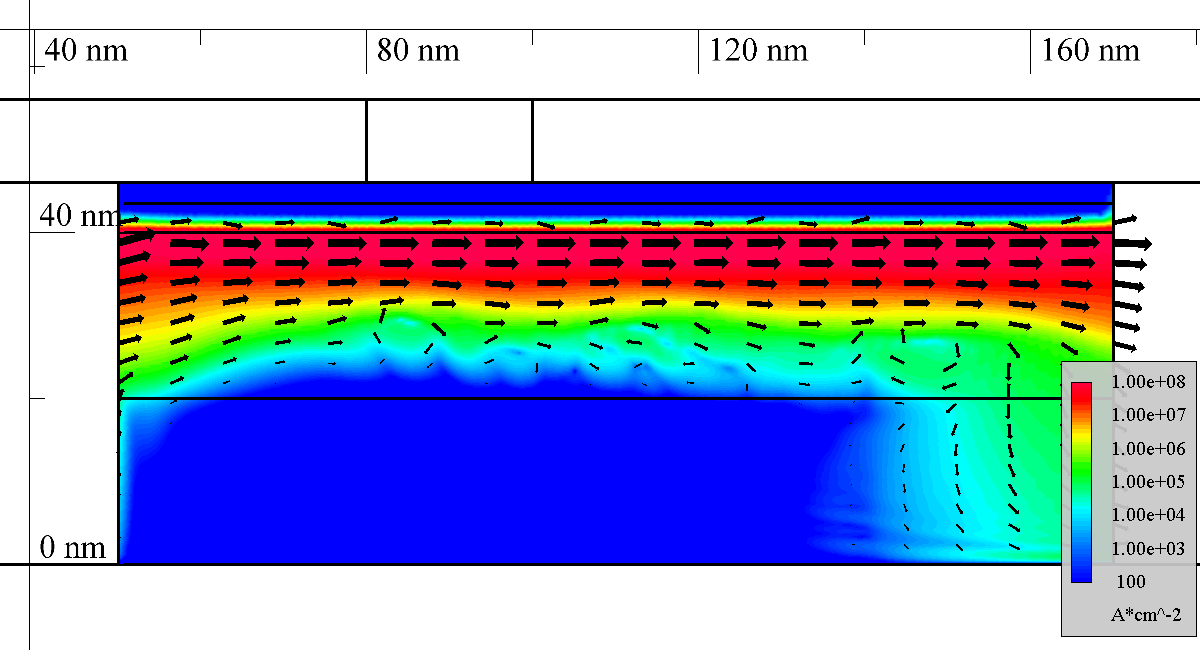
Fig. 1: Self-consistent electron current density in the channel region of the GaN HEMT calculated using the QTBM model at VG = 0V and VDS = 1V; No strain relaxation is assumed and the full piezoelectric charge is taken into account. Due to a large interface charge in the fully strained device, strong confinement is achieved.
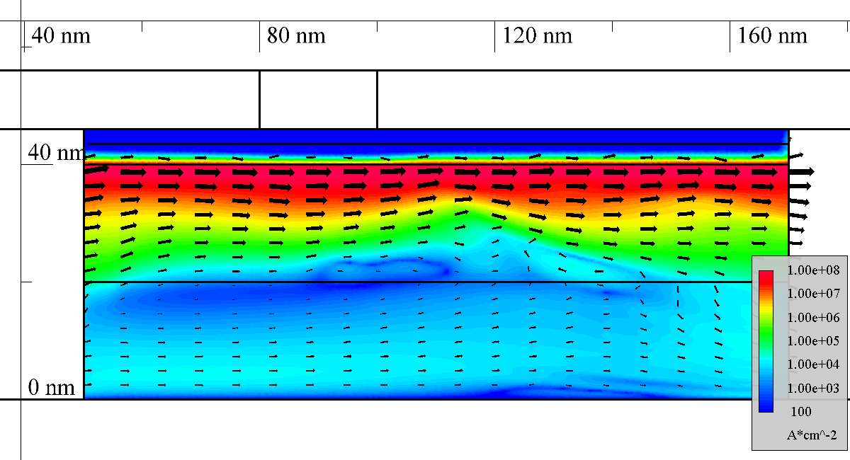
Fig. 2: Same as Fig. 1, but the heterostructure is fully relaxed and only spontaneous polarization is assumed. In the relaxed device, part of the current is already flowing through the back barrier region at a VDS of 1V.