
 |
|
Biography
Raffaele Alberto Coppeta was born in Torino, Italy, in 1986. He studied material engineering at the Politecnico of Torino, where he received the bachelor's degree in 2009 and the master's degree in 2011. He joined the Institute for Microelectronics in 2012, where he is currently working on his doctoral degree. His scientific interests include thermo-mechanical stress modeling using the finite element method for GaN-on-Si chips.
Dislocation Modeling in GaN-Based Devices
Due to the lack of a suitable native lattice matched substrate, gallium nitride based devices are grown upon foreign substrates causing the development of a high density of dislocations which damage the performance of the devices. In order to achieve desired specifications, it is necessary to reduce the dislocation density by using multilayered structures with varying geometry and composition. Defining design rules is necessary to improve the crystalline quality, i.e., to reduce the dislocation density, of gallium nitride based structures. Continuum theory of dislocations treated within the linear elasticity theory and the laws of thermodynamics are used for gaining understanding and modeling the dislocation development in these structures. Our models consider both different types of dislocations, with their specific reactions and inclinations, and also their glide along the interfaces. The results of our calculations show that the glide increases the probability of reactions among dislocations, reducing their density. The reduction is generally small (10% - 15%) for a bilayer structure but can be magnified in multilayer structures. Furthermore, the glide of the dislocations along one interface happens in a short range of tens of nanometers after the critical thickness while the effect of the inclination angle is more evident after hundreds of nanometers after the critical thickness. The higher the inclination angle, the lower the final dislocation density. According to our results, the island-growth mode seems to favor the inclination of the dislocations. Our calculations show that (AlN/GaN)x superlattice structures reduce the dislocation density more efficiently than the Al(1-x)GaxN step-graded layer because the former reduce the dislocation density by nearly one order of magnitude when the thickness of the structure is half μm, yielding a good agreement with experimental data (see Fig. 1). The efficiency of the superlattice is due to the high number of interfaces and the high lattice mismatch between layers. The higher the lattice mismatch, the more effective the dislocation glide.
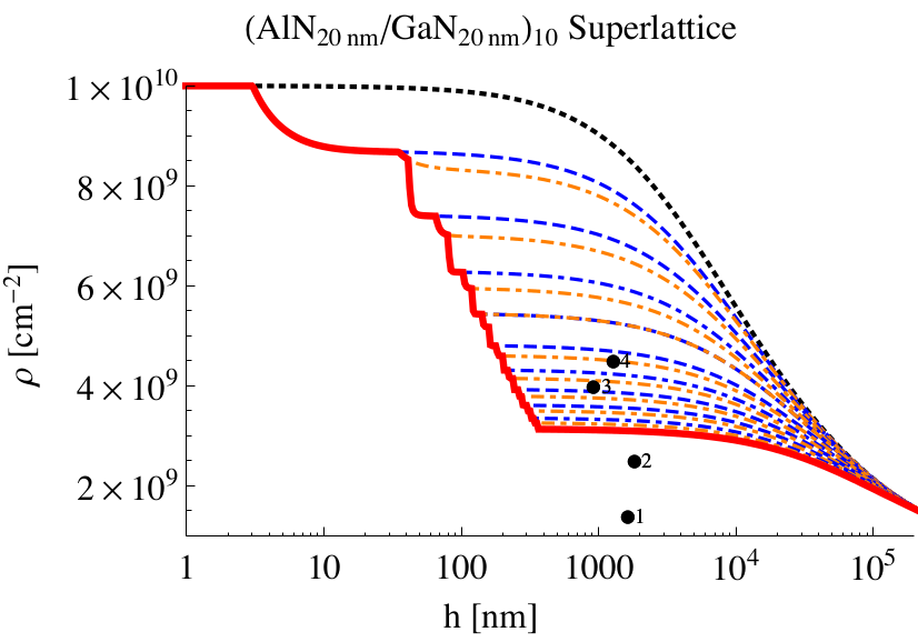
Fig. 1: The red line shows the dislocation density, calculated using our model, as a function of the thickness h of the (AlN/GaN)10 superlattice grown upon an AlN substrate. The dashed lines show the dislocation density using a superlattice with a lower number of layers. The black dotted line shows the dislocation density for a GaN film grown upon an AlN substrate. The theoretical results are compared to experimental data (black dots).