 |
|
Biography
Lado Filipovic was born in Sarajevo, Yugoslavia in 1983. He studied electrical engineering at Carleton University, in Ottawa, Canada, where he received the degree of Bachelor in Electrical Engineering (2006) and Master in Applied Science (2009). He joined the Institute for Microelectronics in January 2010, where he completed his doctoral degree in December 2012. His scientific interest is focused on topography simulations of novel semiconductor processes and the effects of process variability on semiconductor geometries.
Influence of Equipment Variation on the Fabrication of TSVs
Due to the increasing demand for "more than Moore" integration, which combines more on-chip functionality and applications beyond memory and logic, three dimensional integration has become essential. This vertical integration has been facilitated through the use of a Through Silicon Via (TSV), a promising technology which allows for the fabrication of systems connecting various technologies, dense device packing, lower power consumption, and reduced resistive capactive delay. However, a sequence of sensitive processing steps are required in order to generate a TSV with a desired size and aspect ratio. In addition to the deposition of insulation and conducting materials, a method to etch highly vertical trenches through the silicon wafer is necessary. This etching step is carried out using the deep reactive ion etching process, alternatively known as the Bosch process. This process requires the implementation of multiple cycles of deposition and etch steps, which results in a highly vertical trench with rouch, scalloped sidewalls. The exact geometry and thereby the functionality of the final device depends greatly on the process conditions set by the available equipment. There are several ways in which the equipment required for the etch and deposition cycles causes variation in the TSV fabrication process: (1) the valves which are used to push a desired gas into the chamber are not exact and the resulting gas concentration in the chamber can vary by up to 10%; (2) the time required for each step in a cycle is very sensitive, especially since very small time steps are used during these processes in order to ensure a fast overall processing time (the time required for an individual step can vary by 5-15%); and (3) the distribution of the relevant gas along the surface of the wafer is not even. The deposition or etch rate is determined by the fluxes of the relevant molecules and ions flowing at the wafer surface. However, the fluxes are not evenly distributed along the wafer, meaning that a device fabricated in the middle of the wafer functions much differently than one found on the wafer edge. In Fig. 1, the dependence of the radial position of a TSV on its capacitance is shown when the variation of neutral and ion fluxes in the chamber are taken into consideration during the deposition of the isolation oxide on the TSV sidewalls.
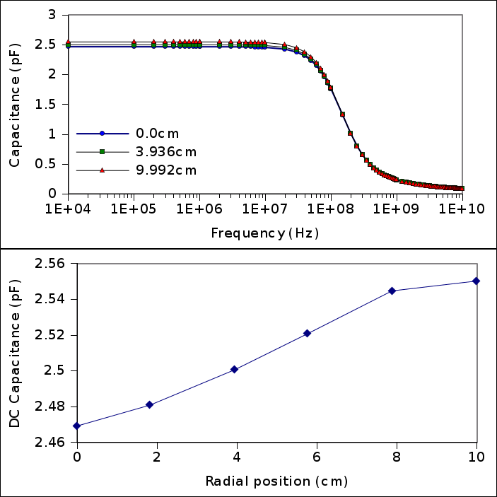
Fig. 1: Simulated capacitance between the metal layer of an open TSV and the silicon wafer. The top figure shows the frequency dependence of the capacitance and the bottom figure shows the dependence of the radial position on the capacitance at 0Hz.