
 |
|
Biography
Tibor Grasser was born in Vienna, Austria, in 1970. He received the Diplomingenieur degree in communications engineering, the PhD degree in technical sciences, and the venia docendi in microelectronics from the Technische Universität Wien, in 1995, 1999, and 2002, respectively. He is currently employed as an Associate Professor at the Institute for Microelectronics. Since 1997 he has headed the Minimos-NT development group, working on the successor to the highly successful MiniMOS program. He was a visiting research engineer for Hitachi Ltd., Tokyo, Japan, and for the Alpha Development Group, Compaq Computer Corporation, Shrewsbury, USA. In 2003 he was appointed head of the Christian Doppler Laboratory for TCAD in Microelectronics, an industry-funded research group embedded in the Institute for Microelectronics. His current scientific interests include circuit and device simulation, device modeling, and reliability issues.
Volatility as a Clue to the Chemical Nature of Oxide Defects
The first observation that oxide traps are more complicated than assumed in simple two-state models (neutral vs. charged) was made twenty-six years ago in Random Telegraph Noise (RTN) studies. There it was observed that the RTN signals could occasionally disappear and reappear, a phenomenon termed anomalous RTN. Although this anomaly was only observed in 4% of the defects, it was suspected that this relatively small number was primarily due to experimental restrictions and that in fact a much larger number of defects could be affected. Similar observations related to disappearing and reappearing defects have been recently made in the context of the Bias Temperature Instability (BTI). This is because charge traps responsible for RTN also form a significant contribution to BTI. In particular, it has been shown by several groups that upon repeating charging and discharging cycles, the average number of active oxide defects in large-area devices can decrease, particularly under harsher stress conditions. However, the detailed dependencies and the nature of the chemical reactions leading to this defect volatility have not yet been explored. Furthermore, NBTI stress was suggested to increase the noise level in large-area devices, presumably by increasing the number of active traps producing RTN. On the other hand, in small-area devices NBTI stress can both increase and decrease the number of defects producing RTN.
In our recent single-defect Time-Dependent Defect Spectroscopy studies, we have already repeatedly come across disappearing and reappearing defects, which have now been studied systematically. The rich spectrum of experimentally observed features includes the following (see also Fig. 1):
(i) Most defects showed volatility, ranging from relatively fast changes (kiloseconds on average) up to many weeks (and probably longer if we had taken more time to wait);
(ii) Even though the activation/deactivation times were found to be relatively large and therefore the number of recorded events small, the process seems to be consistent with a reaction-limited process;
(iii) Defects can become temporarily inactive both in a neutral and a positive state. From that temporarily inactive state, some defects may be activated for instance by a bias pulse toward accumulation (electron injection);
(iv) The capture time constants of defects can change, either spontaneously or as a response to a bake step. While it is conceivable that both the capture and the emission time of a defect change, identification of such a scenario is more difficult, since the emission time is a primary fingerprint in spectral maps;
(v) And finally, defects can permanently disappear, both into a neutral and a positive state. Once disappeared, it may be possible that the defect is reactivated either by a bake step or by chance/spontaneously. However, in some cases even a larger number of bake steps was not able to reactivate the defect. Whether this a consequence of insufficient baking (too short or with a too low temperature), or another fundamental effect remains to be clarified.
In summary, it was found that most defects responsible for the recoverable component of BTI can show volatility. The number of defects showing volatility appears to increase significantly when the device is occasionally driven towards accumulation. The wide range of observed changes at the defect sites could be explained by invoking interactions of hydrogen with precursors in the SiO2 network, whereby the hydrogen is preferentially released by those accumulation sweeps. While the impact of volatility may average out in large devices, characterization of the initial defect configurations in nano-scale devices such as SRAM cells can only provide a snapshot of the current state, and the impact of volatility and transformations must be considered.
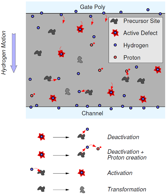
Fig. 1: Simplified schematics of some relevant processes. Not shown is the fact that all defect sites are different. Nuclear reaction analysis demonstrates that hydrogen moves from the gate towards the channel during NBTI stress. Not shown are the interface states created at the channel interface during long-term stress.