 |
|
Biography
Alexander Grill studied Microelectronics at the Technische Universität Wien, where he recieved his Diplomingenieur degree in 2013. Since March 2013 he is working on his doctoral degree at the Institute for Microelectronics. His scientific interests are the simulation of nitride-based heterostructure devices.
Threshold Voltage Drift in GaN-Based MIS-HEMTs
III-V Nitride materials, especially Gallium Nitride (GaN)-based devices, have been found to be good candidates for high-power, high-frequency and high-temperature applications. The reason behind this is that the GaN material system has some major advantages when compared to other materials. The first advantage is the large bandgap, which allows for the design of power devices with very high breakdown voltages. The second advantage is the ability to design heterostructures using Aluminum or Indium doped barrier layers. The large spontaneous and piezoelectric polarization values lead to very high sheet carrier densities at the heterointerfaces, which enables the design of High-Electron Mobility Transistors (HEMTs) with high-power, low on-state resistance and fast switching dynamics.
Despite those superior material properties, widespread applications of GaN based devices are currently limited to laser diodes and microwave power transistors based on Schottky gates. In contrast to Schottky gates, devices with a gate dielectric have lower parasitic gate leakage currents and are a promising platform to design normally-off devices. Unfortunately, especially in the forward bias region these devices still suffer from severe threshold voltage (Vth) instabilities (see Fig. 1).
The main goal of current reliability investigations is to identify the mechanisms responsible for Vth drift. Despite recent efforts to characterize the traps responsible for the Vth drift, their origin and their electrical and physical properties are still a matter of debate. While measurements show very fast drifts with a broad range of time constants, the dynamic behavior cannot be explained entirely by intrinsic properties of different types of traps. The first reason can be identified by the fact that due to the amount of drift, the surface voltage is heavily dependent on the number of trapped charges. This coulomb charging of the dielectric interface dynamically changes the time constants of interface, bulk and oxide traps relative to their equilibrium state. Another effect is the availability of free carriers at the interface. Depending on the bias conditions, the carrier concentration at the dielectric interface can change from deep depletion to deep accumulation. Thus, the dynamic transport of carriers from the channel towards the interface potentially also influences the overall drift behavior. Especially at low temperatures and with moderate gate stress, it can be seen that also the barrier can act as a rate limiting factor for Vth drift.
The modeling of the physical nature of the involved traps, their dynamic behavior and the transport of electrons from the channel to the traps, are the central tasks of our current research activities.
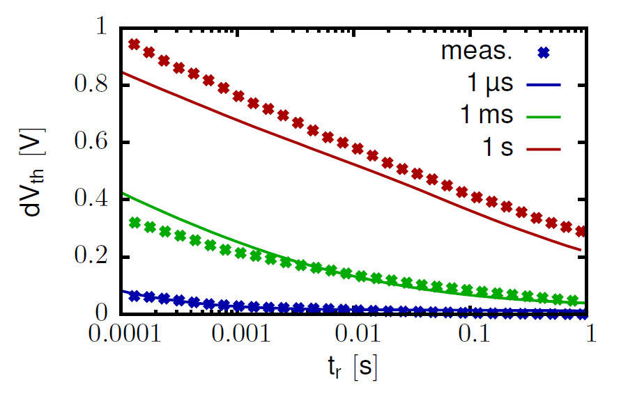
Fig. 1: Recovery transients for 3V single-pulse gate stress with different stress times.