
 |
|
Biography
Yury Illarionov was born in Leningrad (now Saint-Petersburg) in 1988. He studied solid state physics at the Physical Science and Technology Faculty of St. Petersburg State Polytechnical University where he received the BSc and MSc degrees in 2009 and 2011, respectively. From 2010 to 2012 he studied advanced material science in Grenoble Institute of Technology (France) and University of Augsburg (Germany) in frameworks of Functionalized Advanced Materials and Engineering (FAME) Erasmus Mundus program and in September 2012 received a double European MSc degree. His scientific carrier started in October 2007 in Ioffe Physical-Technical Institute (Russia) and in November 2011 he started to work on his doctoral degree there. He also visited IRCELYON (France, May-July 2011) and Singapore Institute of Manufacturing Technology (Singapore, February-July 2012) as a young guest researcher. His previous research was mainly focused on investigation of hot-electron-injection-related effects in tunnel MIS structures with high-k dielectrics. He joined the Institute for Microelectronics in February 2013, where his scientific interests include MOSFET reliability issues, in particular HCD and NBTI.
Investigation of BTI in Double-Gated Graphene FETs
Graphene is considered a promising candidate for applications as a high-mobility channel material in next-generation FETs. In the meantime, graphene FETs (GFETs) are successfully fabricated by different research groups. Therefore, the characterization of their reliability is of great importance. By using subsequent stress/recovery rounds with increasing stress times and constant oxide field, we have performed a detailed study of Bias Temperature Instability (BTI) on the high-k top gate of double-gated GFETs. First, it has been shown that the degradation/recovery dynamics have to be expressed in terms of a Dirac point voltage shift, since the non-negligible Dirac point current shift makes previously used definitions of GFET threshold voltage questionable (Fig. 1). Further it has been found that both Negative BTI (NBTI) and Positive BTI (PBTI) in GFETs can be understood using standard methods previously developed for Si technologies. In particular, the obtained recovery traces for the Dirac point voltage shift can be understood with the Capture/Emission Time (CET) map model (Fig. 2a). However, contrary to Si FETs, only a single Gaussian distribution corresponding to a more recoverable component is required. Nevertheless, the underlying CET distributions (Fig. 2b) closely resemble those known from Si technologies. Moreover, the normalized Dirac point voltage shifts follow the universal relaxation relation, while the corresponding parameters are very similar to those required to fit Si data (Fig. 3). Although the measured defect densities are still noticeably larger than those known from Si FETs, the dynamics of BTI are in general found to be comparable, allowing for quantitative characterization of the graphene/dielectric interface quality. Therefore, a systematic method to benchmark BTI dynamics in GFETs based on the models known from Si technologies is presented.
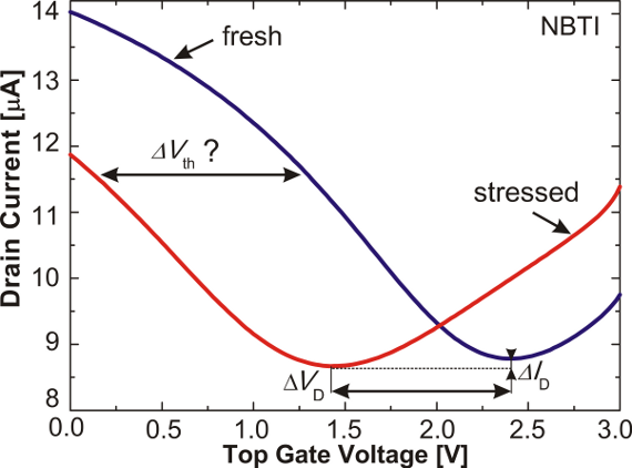
Fig. 1: The typical impact of BTI stress on the top gate results in both a horizontal and vertical shift of the Dirac point. The presence of a vertical drift makes the previously used definition of GFET threshold voltage questionable.
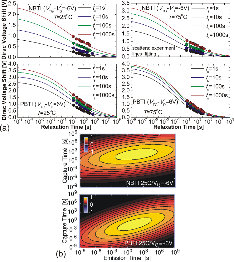
Fig. 2: The Dirac point voltage shift recovery traces for NBTI and PBTI at two different temperatures can be well fitted with the CET map model (a). The underlying Gaussian distributions for time constants closely resemble those of Si technologies (b).
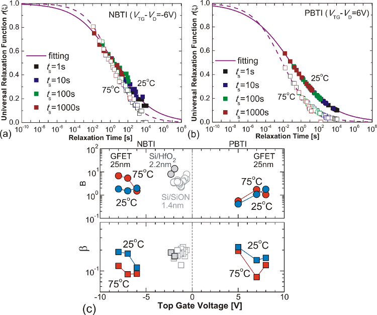
Fig. 3: Both NBTI (a) and PBTI (b) recovery in GFETs follow a universal relaxation relation known from Si technologies. Quite remarkably, the fitting parameters (c) are very similar to their Si counterparts.