 |
|
Biography
Viktor Sverdlov received his MSc and PhD degrees in physics from the State University of St.Petersburg, Russia, in 1985 and 1989, respectively. From 1989 to 1999 he worked as a staff research scientist at the V.A.Fock Institute of Physics, St.Petersburg State University. During this time, he visited ICTP (Italy, 1993), the University of Geneva (Switzerland, 1993-1994), the University of Oulu (Finland,1995), the Helsinki University of Technology (Finland, 1996, 1998), the Free University of Berlin (Germany, 1997), and NORDITA (Denmark, 1998). In 1999, he became a staff research scientist at the State University of New York at Stony Brook. He joined the Institute for Microelectronics at the Technische Universität Wien, in 2004. In May 2011 he received the venia docendi in microelectronics. His scientific interests include device simulations, computational physics, solid-state physics, and nanoelectronics.
Spins in Silicon
With the ability of scaling saturation of CMOS devices to foresee the electron spin, much attention is placed on such devices as a complement or even a replacement of the electron charge in digital information processing. The key advantages of all spin-based computing as compared to a CMOS processor with equivalent functions would be zero standby power, smaller device count, and lower supply voltage and thus dynamic power. Because of weak spin-orbit interaction, the electron spin lifetime in silicon is long, which makes silicon a perfect material for spin-driven applications. Spin injection, detection, and propagation at room temperature were demonstrated recently, however, the nature of several orders of magnitude that are larger than the expected magnitude of the spin accumulation signal in the three-terminal method is still under discussion.
The spin injected in silicon is not conserved and gradually relaxes to zero equilibrium value while diffusing. The electron spin lifetime is determined by the intervalley spin-flip processes. Uniaxial stress along [110] direction lifts the degeneracy between the valleys completely in (001) silicon films. This results in a giant spin lifetime enhancement. Recently, we took into consideration the valley splitting reported in relaxed films which is due to the valley coupling at the Γ point described by a parameter ΛΓ. Inclusion of this additional valley splitting reduces the spin relaxation at the spin hot spots boosting the spin lifetime in unstrained films (shown in Fig. 1). The stress-induced valley splitting, in contrast, moves the hot spots towards unoccupied states, guaranteeing huge spin lifetime enhancement even when the splitting in relaxed films is included. Strain techniques are now routinely used to boost electron mobility. It is straightforward to apply the same techniques to obtain a spin lifetime above 1ns making silicon films and fins perfect spin interconnects.
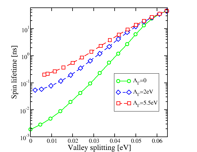
Fig. 1: Spin lifetime as a function of the valley splitting at room temperature in a 2.7nm thin silicon film.