 |
|
Biography
Stanislav Tyaginov was born in Leningrad (now Saint-Petersburg) in 1978. He received his MSc degree in physics (specialization: the physics of semiconductors) in 2002 and his doctoral degree in physics in 2006 (his PhD was devoted to the problem of the impact of insulator thickness non-uniformities on MOS tunnel structure characteristics). He joined the Institute for Microelectronics in January 2008 as a post-doc researcher. His scientific interests include the modeling of HCI-related degradation and TDDB as well as tunneling phenomena in MOS devices.
On the Importance of Electron-Electron Scattering for HCD
The rapid miniaturization of MOSFETs has led to operating voltages scaled below 1V. As a result, Hot-Carrier Degradation (HCD) has evolved from a mode where the damage is produced primarily by solitary hot carriers to a regime in which a substantial contribution is provided by the combined action of multiple colder carriers. In the first case, a bond rupture event can be triggered by a highly energetic carrier. However, if operating/stress voltages are low, this process is unlikely. In scaled devices, the carrier flux can be very high with low average carrier energies. Therefore, several colder carriers which collide with the Si-H bond can substantially excite it (thereby triggering a multiple vibrational excitation mode) and eventually break the bond. As a consequence, HCD appears to be highly sensitive to the way carriers are distributed over energy because high and low energetical particles can trigger different bond dissociation mechanisms. This information is contained in the carrier energy distribution function, which is very sensitive to scattering mechanisms. One such mechanism which plays a crucial role in ultra-scaled devices is Electron-Electron Scattering (EES). EES populates the high-energy tails of the carrier energy distribution function far beyond energies available from the potential drop between the source and the drain. Moreover, Rauch et al. have reported that this mechanism is responsible for severe HCD enhancement in transistors starting from the 180nm node and beyond. Quite to the contrary, the group of Bravaix has suggested that in their devices the role of EES is substantially overestimated in the literature and instead a two-particle mixed mode process drives hot-carrier degradation.
Using our recently developed physics-based HCD model, we investigated the importance of EES in the context of HCD in short- and long-channel transistors. For this purpose we used a series of nMOSFETs of similar architecture but with different gate lengths. We aimed at covering the gate length of 80-100nm at which EES starts to play an important role and thus used the following gate lengths: 44nm, 65nm, 100nm, 150nm, 200nm, and 300nm.
Figs. 1 and Fig. 2 show the experimental change of the linear drain current measured in the devices with gate lengths of 65nm and 150nm stressed at the worst-case HCD conditions and two different drain voltages of 1.8V and 2.2V. To analyse the effect of EES on HCD, we have also plotted degradation traces obtained without EES. One can see that in the case of the 65nm device, ignoring EES leads to a substantial underestimation of HCD also at a relatively low drain voltage of 1.8V. As for the 150nm counterpart, the effect of EES is negligibly weak even at a higher drain voltage of 2.2V. In previous paradigms of hot-carrier degradation, only the channel/gate length was used to judge the importance of EES for HCD. Our findings suggest, however, that a superposition of the device geometry and applied voltages determine whether the effect of electron-electron scattering is strong or not. To check this idea, additional simulations were also performed for the 300nm transistor stressed at the worst-case conditions but at a drain voltage of 2.8V. One can see that if EES is neglected, HCD is overestimated by more than 20%. We conclude thus that the importance of EES is determined by the device topology and the applied stress/operating voltages, i.e., not exclusively by the gate/channel length.
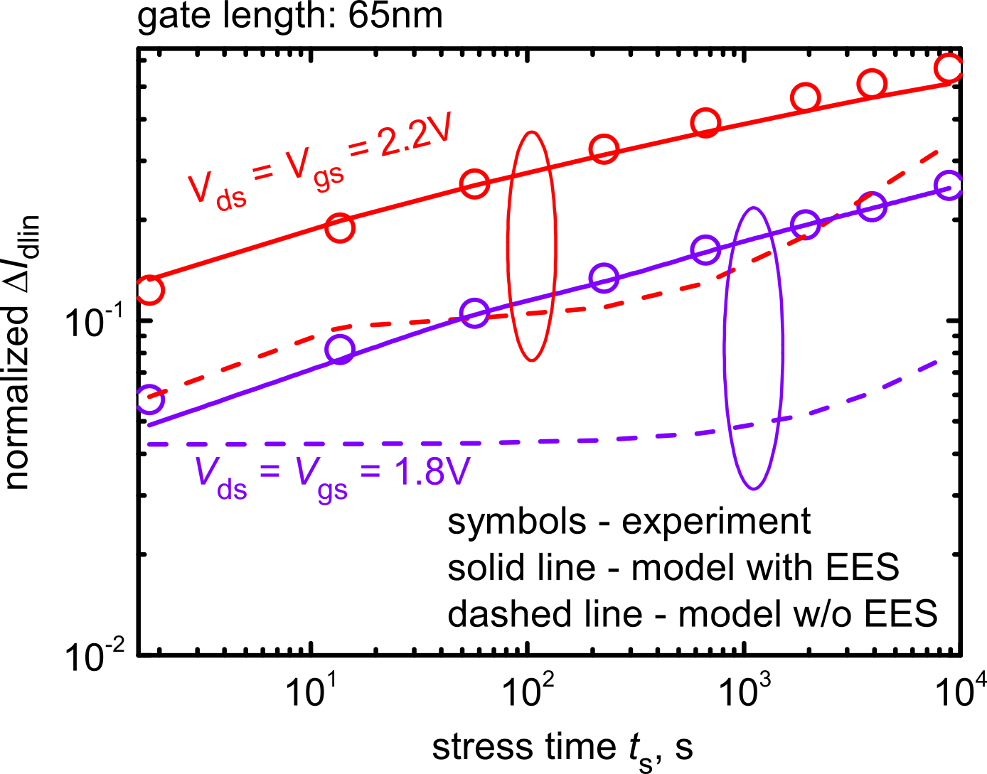
Fig. 1: The normalized change of the linear drain current simulated with and without EES for an nMOSFET with a gate length of 65nm for the HCD worst-case conditions and two different values for the drain voltage: 1.8V and 2.2V. One can see that the effect of EES is substantial for both stress voltages. As a reference, the experimental degradation traces are also shown.
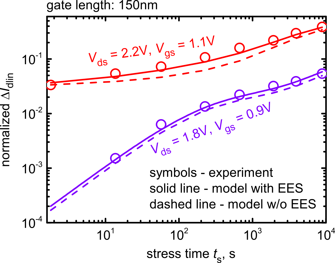
Fig. 2: The same as Fig. 1. but for the 150nm device. In this transistor the EES effect is negligibly weak for both stress conditions.
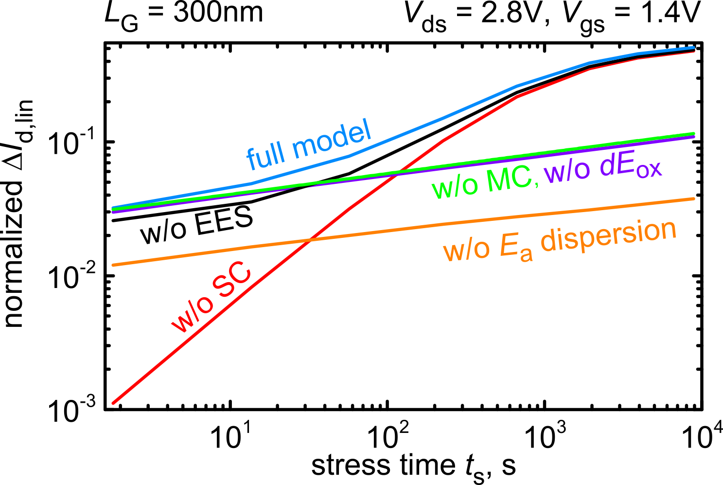
Fig. 3: The linear drain current change vs stress time simulated for the 300nm nMOSFET with the full model and ignoring one of the model components (the two competing mechanisms of the bond rupture, EES, dispersion of the bond-breakage energy, and its reduction by field-dipole interactions). The stress drain voltage is 2.8V. One can see that the effect of EES is strong.