
 |
|
Biography
Michael Waltl was born in Oberndorf near Salzburg, Austria. He received the BSc degree in electrical engineering and the degree of Diplomingenieur in microelectronics from the Technische Universität Wien in 2009 and 2011, respectively. He joined the Institute for Microelectronics in January 2012, where he is currently working on his doctoral degree. His scientific interests include negative and positive bias temperature instabilities and electric measurement methods.
An Advanced Measurement Setup to Study Single Charge Trapping in Nano-Scale MOSFETs
Nowadays MOSFETs have geometrical dimensions in the sub-nanometer regime. In such nano-scale transistors, Bias Temperature Instabilities (BTI) seriously affect device lifetimes. The detrimental impact of BTI on the MOSFETs' performance is caused by defects which are located near the interface or in the oxide. Such defects can interact with the conducting channel by exchanging an electron or a hole which causes a change in device characteristics during operation. From an experimental point of view a particular defect can be identified by its charge capture time, charge emission time, and its step height (i.e., the observed threshold voltage shift). Quite remarkably, in nano-scale devices the carrier exchange events are visible as discrete steps in the drain-source current.
To study the bias and temperature dependence of the capture and emission times of the defects, the recovery after positive/negative bias stress (PBTI/NBTI) is recorded and analyzed (cf. Fig. 1 top). For this an advanced measurement setup has been developed. To analyze the recovery measurement data the Time-Dependent Defect Spectroscopy (TDDS) has been recently proposed and successfully used in numerous studies. In the so called spectral maps, each defect is visible as a cluster with its individual step height and emission time (c.f. Fig. 1 bottom).
The heart of the measurement equipment is our standalone TDDS measure unit. Its modular design offers high flexibility, which is necessary since the system requirements change quickly with the progress in our research. The first module of the setup box allows for the production of a voltage waveform which supports DC and AC voltage signals. Also user defined waveforms or combinations of DC/AC signals followed by defined DC/AC pulses are possible. The output signal frequency can be adjusted up to 1MHz and the output voltage range is +/-5V. Recently, a defined voltage ramp mode has been implemented which is necessary to study permanent device degradation. The second important module is the data acquisition unit which operates at frequencies up to 1MHz. In case of BTI, the device recovery has to be recorded for very long times (up to 10ks and more). To achieve a feasible number of data samples for very long recovery times, the sampling unit supports logarithmically increasing sampling time points. In addition, a high measurement resolution, which is required to record threshold voltage shifts below 0.5mV, is available. Finally, a current-to-voltage (I/V) converter module is used as interface between the waveform generation/sampling unit and the device under test. The I/V converter determines the input current ranges and can be adjusted to currents ranges from 20mA down to 10pA.
So far our sophisticated equipment has already been successfully applied to pMOS and nMOS transistor with SiON and high-k oxides and gate stacks. Furthermore, currently strained SiGe devices are under investigation.
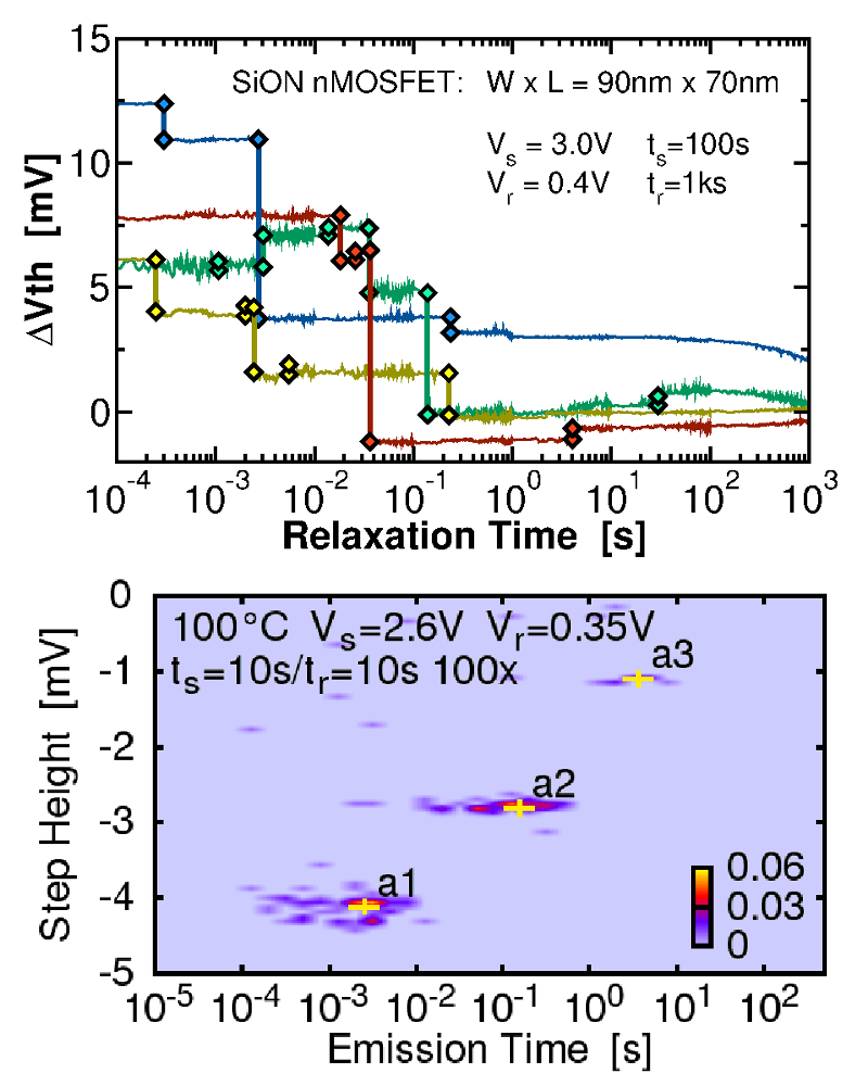
Fig. 1: The four selected recovery traces (top) are recorded with the developed measurement setup from SiON nMOSFETs after DC stress conditions have been applied. Quite remarkably, the measurement delay is below 100us and the minimum detectable step heights is below 0.5mV. The vertical bars show the discrete steps of single emission events. All the steps from 100 measurements of the same stress/recovery conditions are collected in the step height vs. emission time plot. The depicted spectral map (bottom) shows three clusters, which are the fingerprints of the individual defects.