 |
|
Biography
Wolfhard Zisser received the degree of Diplomingenieur in industrial engineering from the Technische Universität Wien in 2011. He joined the Institute for Microelectronics in November 2011, where he is currently working on his doctoral degree. His scientific interests include interconnects, electromigration, and molecular dynamics simulations.
Voiding in Open TSV Structures
Three dimensional integration uses - besides the planar interconnect structures - structures that accomplish vertical connections through the dies. These devices are called Through Silicon Vias (TSVs) and two different approaches are known. The fist is a fully filled cylinder reaching through the die, where the second has a cylindrical form hollow in the middle, therefore the lining is only at the sidewalls of the TSV. Due to the material systems used for the metalization of the considered TSV, a tungsten/aluminum interface is found in the structure. Tungsten in contrast to aluminum has much higher resistance against ElectroMigration (EM) and therefore the interface acts as a blocking boundary for the vacancies driven by EM.
EM induced failure can be distinguished in two phases. In the so called early failure phase the mechanical stress in the structure exceeds a threshold stress and a crack forms in the structure leading to an open circuit failure. In the late failure phase the stress in the structure forms a void, where the resistance changes much less and no failure occurs in the first phase. There a continuing current flow allows the void to move and grow. This movement and especially growth reduces the current conducting cross section and thereby increases the resistance in time. As soon as the resistance reaches a threshold the device fails.
Simulations for the described TSV where carried out. In these simulations first the void free structure was considered to find the locations with the highest probability of void formation. At this location a void was placed and a simulation was carried out based on the phase field model for the tracing of the void surface. For every time step the resistance of the overall structure was calculated and compared against a threshold resistance to find the Time To Failure (TTF) of the TSV for different electrical currents. Fig. 1 shows the resistance increase in time with the typical open circuit behavior at the end of the simulations. This simulation gives the ability to predict both the TTF of interconnect structures due to EM and how those structures can be modified to increase the TTF.
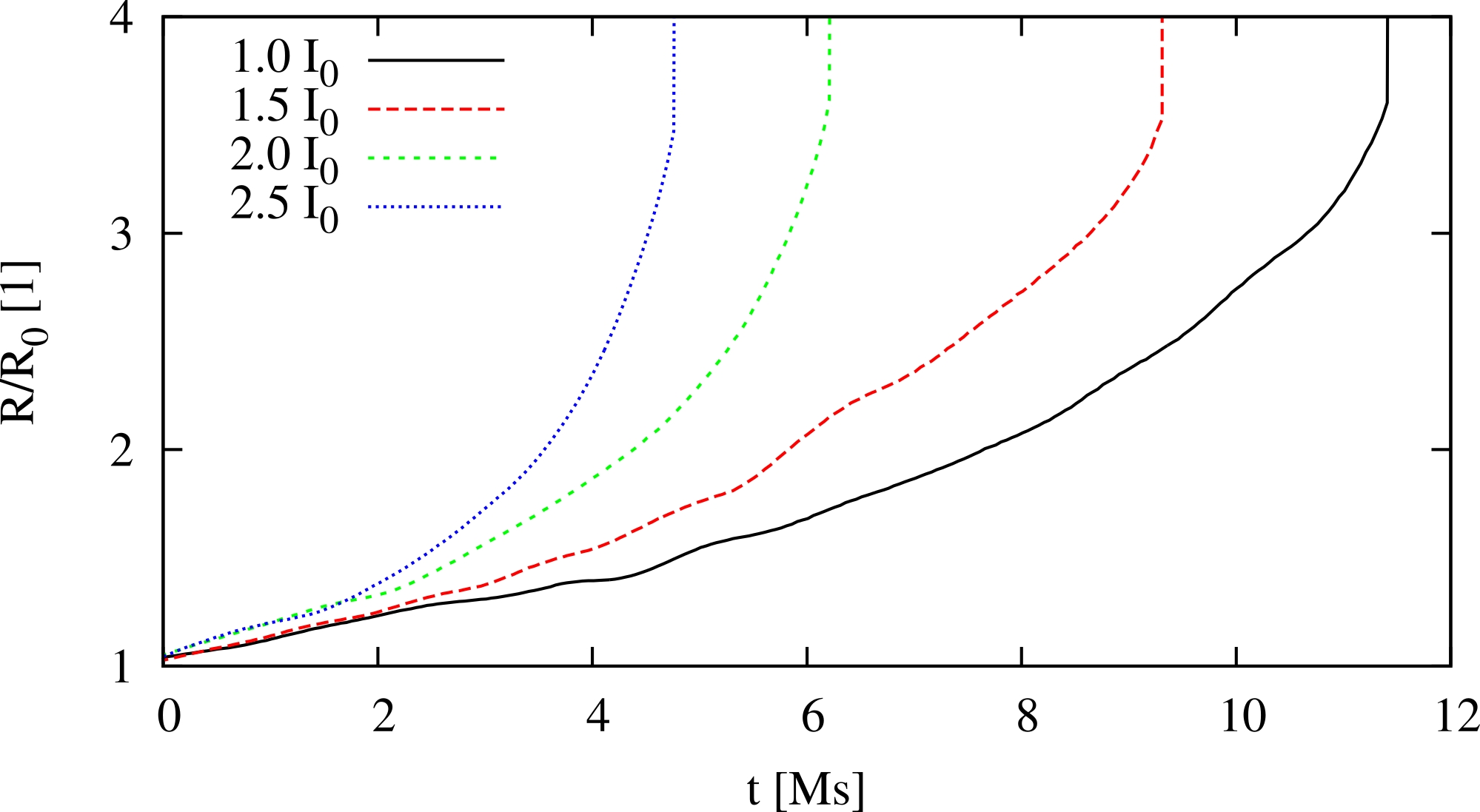
Fig. 1: Resistance increase in time due to EM for different currents.