 |
|
Biography
Hajdin Ceric was born in Sarajevo, Bosnia and Herzegovina, in 1970. He studied electrical engineering at the Electrotechnical Faculty of the University of Sarajevo and the Technische Universität Wien, where he received the degree of Diplomingenieur in 2000. In 2005 he received his PhD in technical sciences and in 2015 his venia docendi in microelectronics from the Technische Universität Wien. In 2010 he was appointed the head of the Christian Doppler Laboratory for Reliability Issues in Microelectronics. He is currently an Associate Professor at the Institute for Microelectronics. His research interests include modeling and simulation of reliability issues in interconnects for ultra large-scale integration.
TCAD Methods for the Study of Reliability and Performance of Nano-Interconnects
With each new generation of modern integrated circuit, the density and complexity of on-chip interconnects increases. Consequently, the cross-section of the interconnect decreases while, at the same time, supply voltage for transistor and interconnect systems does not scale proportionally, resulting in an increase of current densities. Smaller interconnects now pose a significant delay to signal propagation in a chip and are much more susceptible to reliability issues. Metal damage caused by current-carrying electrons, termed electromigration, is one of the main reliability issues for modern interconnects. Electromigration leads to the formation of voids inside the metal of the interconnect which cause device failure.
When it comes to the fabrication of reliable interconnects with thicknesses between 100 nm and 10 nm, the technological challenges are enormous. The introduction of new metallization schemes usually produces new failure behaviors which are influenced by a multitude of factors. In order to reduce the amount of unintended reliability issues as interconnects are downscaled, engineers must modify the technology process, the selection of materials, and the geometry of the interconnects. Due to the complexity and number of relevant physical effects, many costly experiments are usually needed to determine the set of optimal modifications. Thus, a TCAD approach, which includes simulation and modeling based on the physics of downscaled interconnects, represents a useful source of support and guidance that can reduce both design costs and time.
To investigate the reliability of nano-interconnects, a set of different simulation methods is applied. The first is an ab initio method for the calculation of atomistic electromigration force. As an effect which arises due to electron scattering, electromigration is influenced by the narrow interconnect effect and by the presence of grain boundaries and interfaces. The second method involves continuum simulation of material transport induced by electromigration, which enables the effect of mechanical confinement of the surrounding layers of the interconnects to be investigated. Simulation results obtained by these means enable us to study interconnect degradation as a function of different impact factors, such as choice of interconnect metal, microstructural properties, layout, and operating conditions.
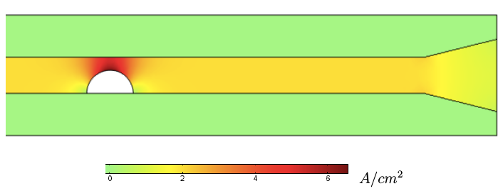
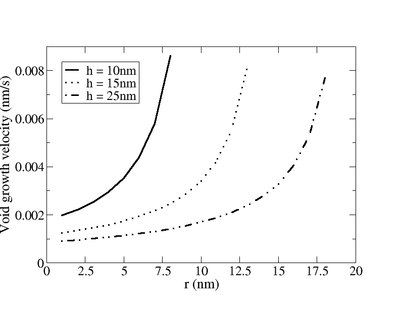
In Fig. 1, a void in the interconnect metal with surrounding current density is presented. The simulation with high gradients of current density needs very fine locally adapted finite element meshes (see Fig. 2), an important factor for reliability and void growth velocity. In Fig. 3, void growth velocity dependence on interconnect thickness and void radius is displayed.

Fig. 1: Current density distribution around a void in a mechanically confined interconnect.

Fig. 2: Finite element mesh in the vicinity of the void structure used for simulation.

Fig. 3: Void growth velocity as a function of the void radius (r) and interconnect thickness (h).


