 |
|
Biography
Markus Jech was born in Vienna in 1986. He received the degree of Diplomingenieur in Physics from the Technische Universität Wien in 2014. In January 2015 he joined the Institute for Microelectronics, where he is currently working on his doctoral degree.
Towards a Unified Model for Bias Temperature Instability and Hot Carrier Degradation
A large number of publications have independently investigated bias temperature instability (BTI) and hot carrier degradation (HCD) modes, but only a few papers report the interplay between these two mechanisms. The link between these degradation modes, however, has gained importance in recent years, since rapid scaling of MOSFETs has led to a change in the worst-case stress conditions for HCD. In early technology nodes, the maximum bulk current observed at VG~VD/2 was recognized as the worst degradation regime, whereas in modern nodes VG = VD is known to be the worst case. In the latter case, BTI is likely to provide a significant contribution of apparent HCD. This is of particular importance for negative BTI in SiON technologies and in general for devices with high-k gate stacks where positive BTI is usually prominent.
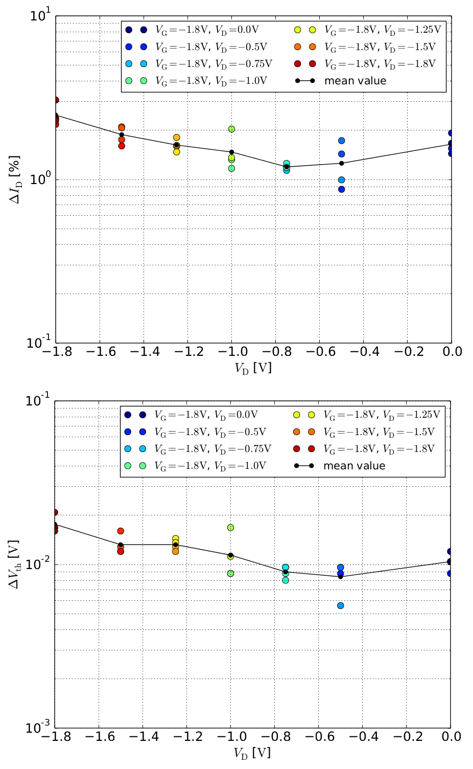
Fig. 1 shows the normalized change of the linear drain current (left panel) and the threshold voltage shift (right panel) after a 1 ks stress phase measured on a 90 nm pMOSFET at T = 125 °C. VG was fixed at -1.8 V, and VD increased from 0 V (pure homogeneous BTI), to VD < VDD (inhomogeneous BTI), and up to VD = VG (mixed HCD and BTI mode). One can clearly see a drift minimum around VD = -0.5 V before the degradation becomes more severe due to the onset of the low energy HCD mode. This initial reduction of BTI degradation is usually explained by the decrease of the channel's vertical electric field under the influence of a drain bias. For a more detailed explanation of this behaviour, however, one also needs to consider the change of the carrier distribution function (DF) with increasing drain voltage. For homogeneous BTI conditions the carriers are in equilibrium and the DFs can be modeled using Fermi-Dirac statistics. This assumption is not valid when a nonzero VD is applied, because the shape of the DF severely changes due to various scattering mechanisms.
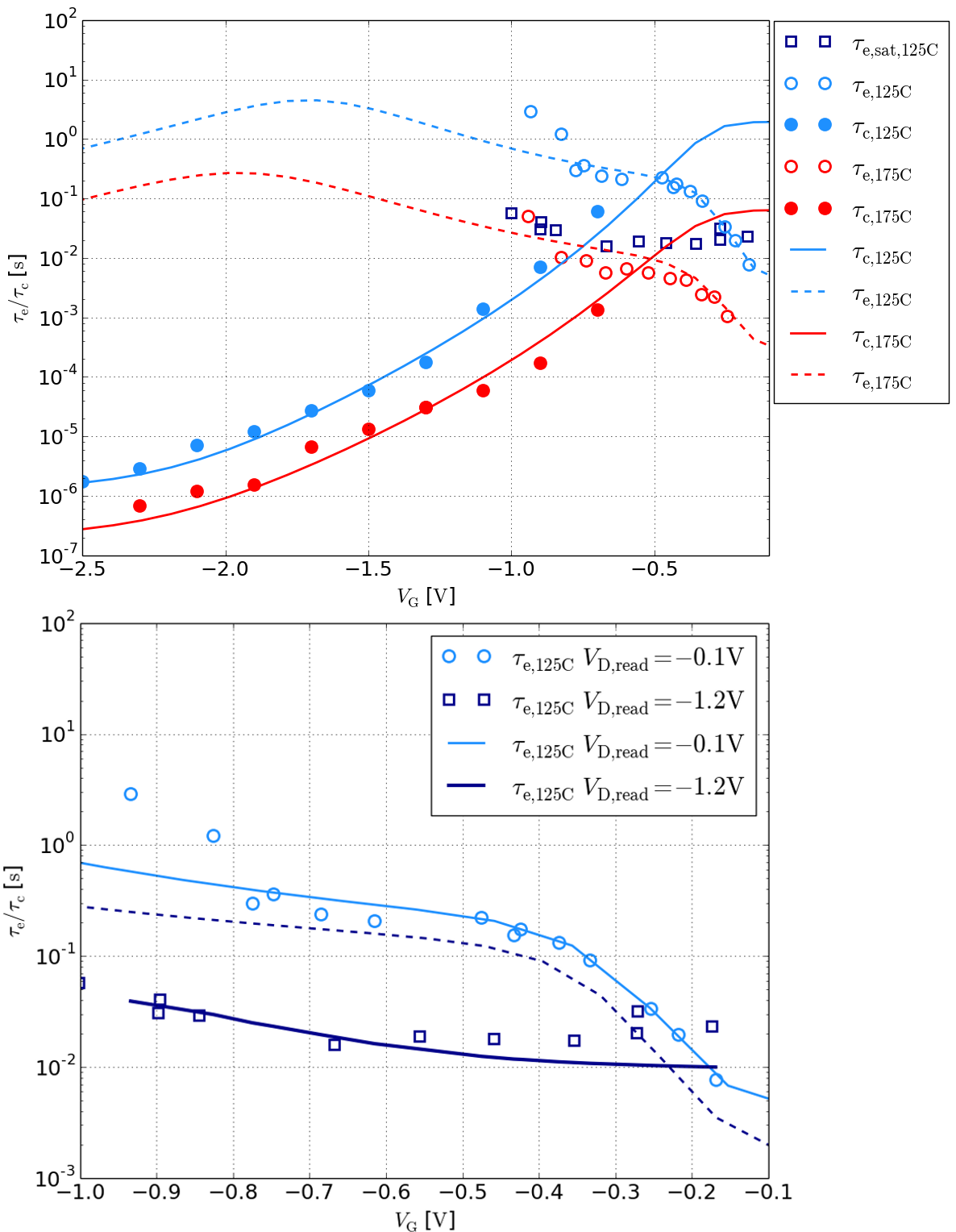
To investigate the aforementioned effects and their consequences in more detail, Fig. 2 (left panel) shows the capture and emission times for two different temperatures of an individual bulk oxide trap located in the middle of the channel. Symbols represent experimental data and lines represent simulation results. One can see that the four state non-radiative multiphonon (NMP) model perfectly represents the experimental data. The additional measurement set (squares) describes the emission behaviour for an increased drain voltage during recovery at T = 125 °C. Such a dramatic difference, compared to the characteristics obtained for low VD, cannot be explained by a simple reduction of the electric field. The right panel provides a more detailed picture together with two simulation results. The full simulation (solid lines) includes the effect of non-equilibrium DFs which were used within the NMP model to calculate the characteristic times. Accurate DFs were obtained from a solution of the Boltzmann transport equation using the deterministic solver ViennaSHE. If this crucial component is neglected (dashed line), it is not possible to adequately model the experimentally observed behaviour.

Fig. 1: Threshold voltage drift and normalized change of ID,lin after 1 ks stress for a fixed VG = -1.8 V and varying VD = [0 V, -1.8 V], each stress condition was measured on four different devices. Around VD = -0.5 V a minimum is visible.

Fig. 2: Capture and emission times for an individual oxide defect. A dramatic difference is visible in the emission times for an increased readout voltage during recovery.


