 |
|
Biography
Mahdi Pourfath was born in Tehran, Iran, in 1978. He studied electrical engineering at the Sharif University of Technology, where he received the degree of Master of Science in 2002. He joined the Institute for Microelectronics in October 2003, where he received his doctoral degree in technical sciences in July 2007 and the venia docendi in microelectronics in March 2016. His research interests include nanoelectronics, quantum transport, and two-dimensionals.
Sensitive Strain Gauge Sensors Based on Two-Dimensional Materials
Graphene, as the most prominent 2D material, is attractive for use in next-generation nanoelectronic devices because of its high carrier mobility. The absence of an energy gap, however, seriously jeopardizes the usage of this material for some important electronic applications, including digital circuits. Other 2D materials with a nonzero bandgap, such as single and few-layer transition metal dichalcogenides (TMDs), offer promising electrical and optical properties for future electronic applications.
We have performed a comprehensive analysis on the effect of strain on the mobility of several TMDs (MoS2, MoSe2, WS2, and WSe2), employing ab initio simulations of the band structure and the linearized Boltzmann transport equation for mobility evaluation, including the effects of intrinsic phonons, remote phonons, and screened charge impurities. The lowest- and the second-lowest band minima in the conduction band of these materials are denoted as K- and Q-valleys.
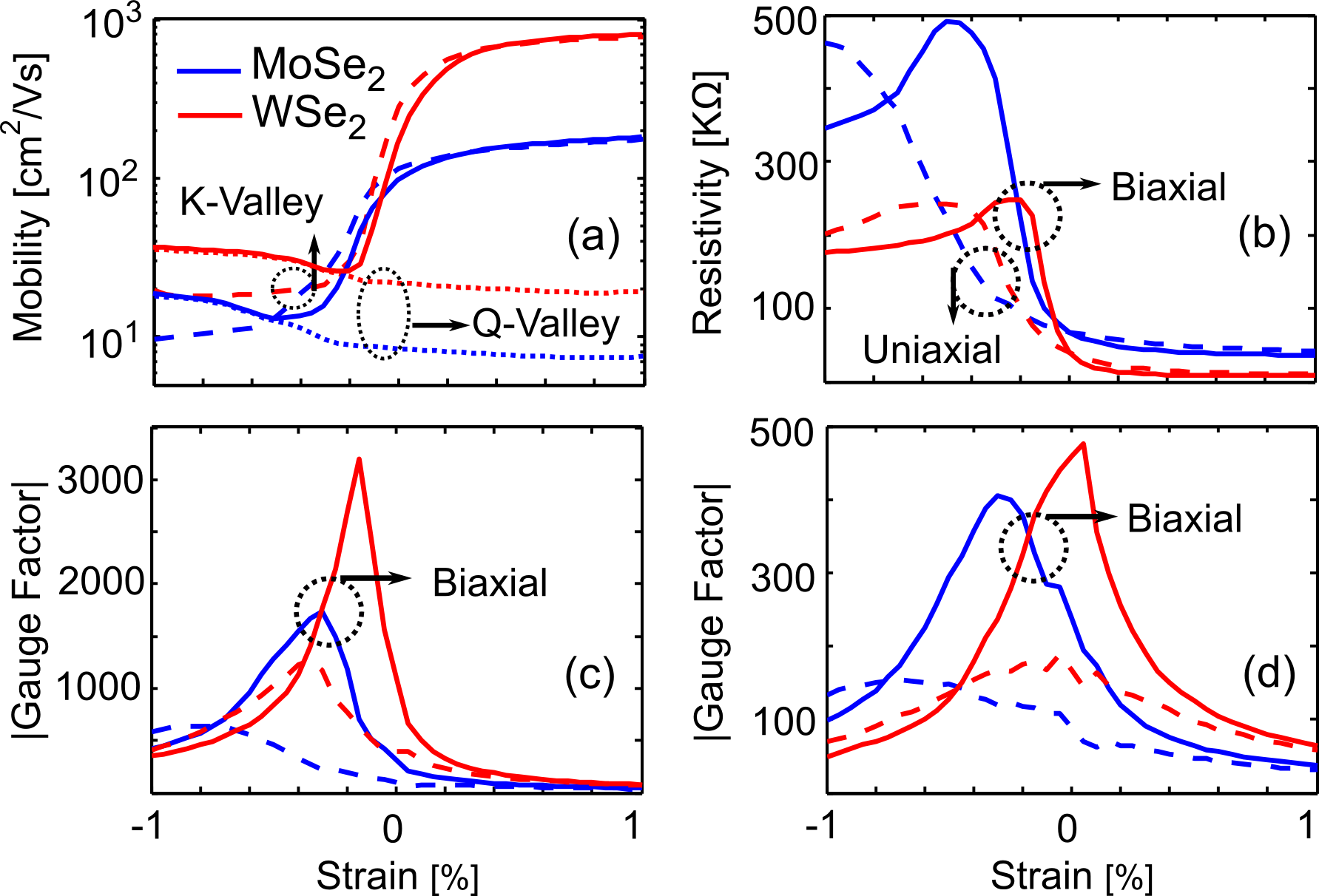
The results indicate that a tensile strain increases mobility, whereas a compressive strain reduces mobility. Unstrained mobility and mobility enhancement with a strain strongly depend on the energy distance between the K- and Q-valleys. A small tensile strain has a higher impact on the mobility of materials with a smaller energy distance between the valleys, such as MoSe2 and WSe2.
Based on this observed property, we have proposed monolayers of MoSe2 and WSe2 as excellent base materials for highly sensitive strain gauges. Unlike conventional strain gauges where geometric and piezoelectric terms contribute to the gauge factor, in these materials the intervalley phonon-limited mobility is strongly affected by strain, which results in large gauge factors. Even in the presence of extrinsic scattering sources, the gauge factors of these materials are much larger than those reported for most of the materials typically used for strain gauges. Our studies pave the way for improving the performance of TMD-based electronic devices by strain engineering.

Fig. 1: (a) The phonon limited mobility as a function of strain: Overall mobility (solid), mobility in K-valleys (dashed), and mobility in Q-valleys (dotted). (b) The resistivities; (c) and (d) the gauge factors as functions of strain. Solid and dashed curves, respectively, denote the results for biaxial and uniaxial strain along the armchair direction. (b) and (c) correspond to results including only intrinsic phonon scattering; results in (d), on the other hand, account for intrinsic phonon, remote phonon, and charge impurity scattering.


