 |
|
Biography
Prateek Sharma was born in Kota (Rajasthan), India. He recieved degree of Master of Science in electrical engineer from Linköping University, Sweden in 2012, where he was also invovled in smart dust and body area networks research projects. He joined the Institute for Microelectronics in March 2013 where he is working on the realiability systems in microelectronics.
The Role of Cold Carriers in Hot Carrier Degradation
The lucky electron model for hot carrier degradation (HCD) assumes that the phenomenon of HCD is dominated by solitary hot carriers with high energies (SC-process). This scenario is considered typical. As for cold carriers, various other models suggest that cold carriers play a role only in ultra-scaled devices. In our recent studies, however, we discovered the important role that both hot and cold carrier populations play in properly modeling HCD in large and high power devices like LDMOS (laterally diffused MOSFET) transistors.
We model the carrier energy distribution function (DF) using a simplified form of the Boltzmann transport equation's (BTE) solution, namely the drift-diffusion (DD) approach. As a reference, we also calculate a solution of the BTE using the spherical harmonics expansion method. The DD-based approach greatly simplifies carrier transport treatment, which is a complicated task in power devices because of their complex structures, large dimensions, and high operating voltages. Thereby, the carrier energy distribution function is approximated by an analytic expression linked to the electric field and the density of carriers found using the DD simulations.
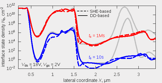
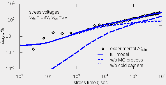
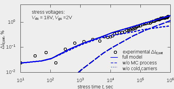
Two ingredients are used to represent the role of cold carriers in our HCD model. First, cold carriers are represented by the corresponding term in the analytic formula for the carrier distribution function. Second, they contribute to the multiple-carrier (MC) processes of Si-H bond dissociation. We check the validity of the model by neglecting the effect of cold carriers in HCD modeling in the case of nLDMOS devices stressed at high voltages. In order to study if the effect of cold carriers can be neglected at such high drain voltages as Vds = 18 V, we have calculated the interface state density Nit(x) profiles without the contribution of the SC-process (Fig. 1), as well as the changes of the linear and saturation drain currents ∆Id,lin(t) and ∆Id,sat(t) (see Figs. 2 and 3).
As can be seen in Figs. 2 and 3, at short stress times, neglecting the cold carrier contribution to DF does not affect HCD, while at times longer than 5 ks, the drain current change is substantially underestimated. This is because short-term HCD is determined by the drain Nit peak, which is already visible at 10 s (see Fig. 1). Suppressing the MC-process contribution leads to HCD underestimation at all stress times. Such a trend is especially pronounced at short stress times. This is due to the fact that even hot carriers, which do not have energy equal to the activation energy required for defect creation, contribute to the MC process. Thus, both single- and multiple-carrier processes of bond dissociation are strongly coupled. So, for a comprehensive HCD model, the populations of both hot and cold carriers are important, even for large devices and high voltages.

Fig. 1: Interface state density profiles obtained with SHE- and DD-based models for the nLDMOS transistor, without the effect of the MC-process at stress times 10 s and 1 ms. The case where all the superpositions of SC- and MC-processes are considered in the DD-based model is also plotted for comparison (grey lines).

Fig. 2: The change of the linear drain current as a function of stress time: Experimental data, the results of the full model, and the traces obtained neglecting the cold carrier term in DF and without the MC process.

Fig. 3: The same as Fig. 2 but for the saturation drain current.


