 |
|
Biography
Stanislav Tyaginov was born in Leningrad (now Saint-Petersburg) in 1978. He received his MSc degree in physics (specialization: the physics of semiconductors) in 2002 and his doctoral degree in physics in 2006 (his PhD was devoted to the problem of the impact of insulator thickness non-uniformities on MOS tunnel structure characteristics). He joined the Institute for Microelectronics in January 2008 as a post-doc researcher. His scientific interests include the modeling of HCI-related degradation and TDDB as well as tunneling phenomena in MOS devices.
Understanding and Modeling the Temperature Behavior of Hot-Carrier Degradation
The temperature behavior of hot-carrier degradation (HCD) has been shown experimentally to change when the dimensions of transistors are scaled down. In long-channel devices, HCD is suppressed at elevated temperatures, while in short-channel devices, it typically becomes more severe at higher temperatures. Summarizing available experimental data, one concludes that this transition occurs at channel lengths of around 100 nm.
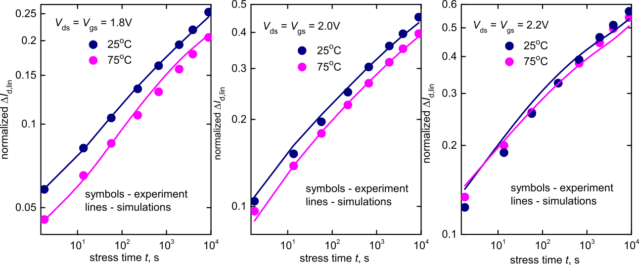
Within this context, our measurements, quite intriguingly, have directly shown that, even in SiON nMOSFETs with a gate length of 65 nm, the change of the linear drain current, ∆Id,lin(t), recorded during hot-carrier stress, is lower at higher temperatures (see Fig. 1). One can see that for low drain (Vds) and gate (Vgs) voltages, Vds = Vgs = 1.8 and 2.0 V, the ∆Id,lin values for T = 25 °C are higher than those for T = 75 °C. This result contradicts previous findings obtained in transistors with comparable gate lengths. Also, the distance between ∆Id,lin(t) curves reduces as Vds and Vgs increase, and at Vds = Vgs = 2.2 V, the ∆Id,lin values are almost the same for both temperatures within the whole stress-time slot.
We assume that HCD is driven by the generation of interface traps due to the dissociation of pristine Si-H bonds at the interface. The Si-H bond is described within the truncated harmonic oscillator model. Bond rupture is modeled as a superposition of the multiple vibrational excitations (MVE-process) of the bond by carriers with a total energy smaller than the bond-breakage activation energy, Ea, and hydrogen release induced by a solitary hot-carrier (AB-process). The electron energy distribution functions (DFs) simulated for the aforementioned stress conditions show that for low and moderate energies, the DF values are higher at 25 °C, while the high-energy tails are more populated at 75 °C. Such behavior allows us to conclude that the MVE-process rate should be higher at 25 °C, while the AB-process rate increases with temperature. Another factor which determines the impact of temperature on the MVE-process kinetics is the vibrational lifetime which decreases with T. At higher temperatures, vibrational levels depopulate faster and a higher carrier flux is needed to maintain the bond-breakage rate at the same level.
Fig. 1 shows good agreement between experimental and simulated ∆Id,lin(t) dependencies. To study the interplay between the AB- and MVE-processes in greater detail, we have also simulated HCD traces neglecting the AB-process. These curves show that if the AB-process is ignored, the distance between the ∆Id,lin(t) curves evaluated at 25 °C and 75 °C dramatically increases. Even in the case of Vds = Vgs = 2.2 V, hot-carrier degradation is still weaker at 75 °C. This is because, in this artificial case, hot-carrier degradation is driven by the MVE-process, the rate of which reduces with T. In other words, the temperature behavior of HCD is determined by the interplay between the AB- and MVE-mechanisms. At lower stress voltages (Vds = Vgs = 1.8 and 2.0 V), HCD is driven by the MVE-mechanism. Thus, ∆Id,lin values are weaker at higher T. The contribution of the AB-process increases, however, with the applied voltage, and at Vds = Vgs = 2.2 V the AB-mechanism becomes dominant. The different temperature dependences of the AB- and MVE-processes therefore compensate for each other, and the ∆Id,lin values are almost the same at both 25 °C and 75 °C.
Note finally that HCD itself is a very complex phenomenon that cannot be described by a single process. For a proper description, which is valid for different technologies, the interplay between various mechanisms ought to be considered. We have shown previously that even in long-channel and/or high-voltage devices, one cannot neglect the contribution of electron-electron scattering and the multiple-carrier process of bond dissociation. On the other hand, the single-carrier mechanism plays a significant role also in decananometer devices. The same holds true for the intricate temperature behavior of HCD. Only after all the effects are taken into account and combined with the temperature-dependent vibrational lifetime can the true temperature characteristics of HCD be revealed.

Fig. 1: The experimental changes of the linear drain current as a function of stress time, ∆Id,lin(t), compared against simulation results for three different combinations of stress voltages (Vds = Vgs = 1.8, 2.0, and 2.2 V) and two different temperatures (25 °C and 75 °C). One can see that the distance between the ∆Id,lin(t) curves obtained for 25 °C and 75 °C decreases as Vds and Vgs increase. For Vds = Vgs = 2.2 V, however, the ∆Id,lin values remain almost the same through the entire stress-time window. Agreement between both experimental and simulated ∆Id,lin data is very good.


