 |
|
Biography
Michael Waltl was born in Oberndorf near Salzburg, Austria. He received the BSc degree in electrical engineering and the degree of Diplomingenieur in microelectronics from the Technische Universität Wien in 2009 and 2011, respectively. He joined the Institute for Microelectronics in January 2012, where he is currently working on his doctoral degree. His scientific interests include negative and positive bias temperature instabilities and electric measurement methods.
Superior NBTI Reliability in High-k SiGe Transistors
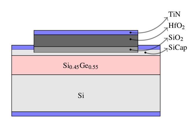
In modern high performance CMOS applications, nanoscale high-k transistors are used routinely. In such devices, however, negative bias temperature instabilities (NBTI) pose a serious threat to further device scaling. A possible solution to this problem is the introduction of a thin SiGe channel, which acts as a quantum well, together with a Si-cap layer below the high-k gate stack (see Fig. 1). To study the impact of NBTI in nanoscale SiGe devices, we employ the recently proposed time-dependent defect spectroscopy (TDDS) framework. For our investigation of large area devices, we have used an extended measure-stress-measure scheme. To investigate the microscopic reasons for improved reliability with respect to NBTI caused by the Si-cap layer, two device variants with different Si-cap layer thicknesses are compared to a Si reference device.
So far, in nanoscale devices, the TDDS has been successfully applied to experimentally characterize individual traps by their bias- and temperature-dependent capture/emission time characteristics as well as by their step heights. Subsequently, the device simulator Minimos-NT and the four-state non-radiative multiphonon (NMP) model are used to analyze device electrostatics and to explain the observed capture/emission time characteristics of a number of individual traps.
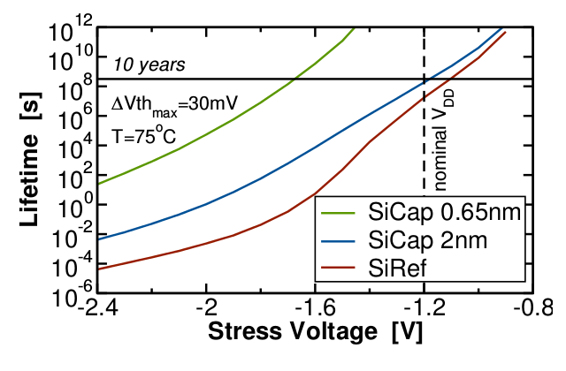
Furthermore, the response of large area devices subjected to NBTI stress has been studied intensively. Based on the NMP parameters set from previous single-trap investigations, a large number of traps with widely distributed NMP trap parameters are used to explain the measured recovery behavior for certain stress/recovery biases and times at different device temperatures. Based on these simulations, the lifetimes of SiGe devices with different Si-cap layer thicknesses can be estimated. As shown in Fig. 2, the introduction of a thin Si-cap layer together with a SiGe channel leads to a massive decrease in the device's sensitivity to NBTI stress, thereby boosting the lifetime of the device.

Fig. 1: Schematic view of the SiGe channel devices shows the high-k gate stack together with the thin Si-cap layer and the SiGe channel.

Fig. 2: At a nominal operating voltage of VDD = -1.2 V, a lifetime of more than ten years is easily achieved for the SiGe devices.


