 |
|
Biography
Wolfhard H. ZISSER received the degree of Diplomingenieur in industrial engineering from the Technische Universität Wien in 2011. He joined the Institute for Microelectronics in November 2011, where he received his doctoral degree in 2016. His scientific interests include interconnects, electromigration and SOI structures.
Plastic Deformation of SOI Wafers
Silicon on insulator (SOI) wafers consist of a substrate made out of single crystal silicon, an insulating oxide layer on the substrate, and a silicon layer bonded on top of the oxide. The silicon oxide and the SOI layers have thicknesses in the range of tenths of micrometers and are therefore quite small compared to typical wafer diameters, which are in the range of hundreds of millimeters. This makes simulations based on the finite element method (FEM) challenging since high mesh quality is crucial when it comes to obtaining meaningful results.
Warping of SOI wafer structures can lead to focusing problems during fabrication. The understanding of elastic deformation, as well as plastic deformation, during processing is therefore of major interest. Deformations are triggered due to stress introduced by three mechanisms. The first mechanism is a bending of the wafer due to gravity. This introduces a shear stress at the top of the wafer and a tensile stress at the bottom. Furthermore, additional stress is introduced around the wafer’s mechanical supports inside the furnace. The second mechanism is triggered by the difference in the coefficients of thermal expansion between pure silicon and silicon oxide during the heating and cooling processes. The third mechanism is caused by an inhomogeneous temperature distribution during boat-in and boat-out. Silicon undergoes a brittle-to-ductile transition in the furnace during processing. In the wafer, a plastic deformation can therefore occur, leading to irreversible deformations.
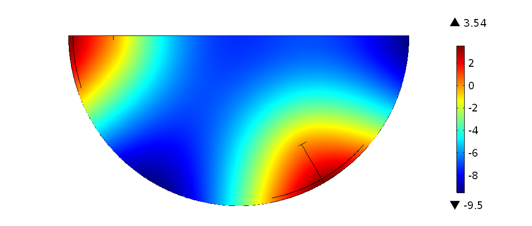
In Fig. 1, the displacement of a wafer due to gravity is shown. For the wafer, the roller boundary condition is employed in order to reduce required meshing elements by one half. This reduction decreases computation time, as well as memory requirements. The wafer is placed on three pins located at a separation angle of 120°. In this project, FEM-based mechanical models, including crystal dislocation dynamics as the source of plastic deformations, are implemented. These simulations are intended to help SOI wafer manufacturers predict plastic wafer warping. These predictions will help to design a furnace process, thereby reducing warping to an acceptable amount.

Fig. 1: Horizontal displacement in micrometers of a wafer 200 millimeters in diameter due to gravity.


