 |
|
Biography
Al-Moatasem El-Sayed was born in Sheffield, United Kingdom in 1988. He completed his Masters in chemistry at the University of Manchester in 2010. He went on to do his Ph.D in physics at University College, London, focussing on atomistic modeling of point defects in oxides. He then joined the Institute of Microelectronics in June 2015, his current research interests are modeling of point defects in oxides and their effect on electronic devices.
The Role of Electric Field on Oxide Defect Behavior
The scaling of metal-oxide-semiconductor field-effect transistors (MOSFETs) over the past few decades has brought a number of reliability issues to the fore. Many of these reliability issues implicate point defects in the oxide, the semiconductor and at their interface. For example, models for both the negative bias temperature instability and hot carrier degradation, two well-known reliability issues, are reliant upon charge trapping defects in the oxide.
Many studies have focused on characterizing defects' properties in order to identify those that play a role in reliability issues. Computational modeling offers a spectrum of tools that can be used to analyze point defects. In particular, density functional theory (DFT) implemented in highly parallelized codes has been widely used to identify and develop models of point defects in oxides. Using the CP2K code, we have shown that hydrogen atoms can interact with strained Si-O bonds to form defective sites in a-SiO2.
These results clearly demonstrate that the amorphous material’s structural disorder can actually cause atomic hydrogen to have a detrimental effect, in stark contrast to its well-known healing properties. Hence, atomic hydrogen is not always a benign agent when processing SiO2 and can actually produce thermodynamically stable neutral defects in a-SiO2, adding to the density of dangling bond defects, such as E' centers, which are implicated in reliability issues of devices that utilize a-SiO2.
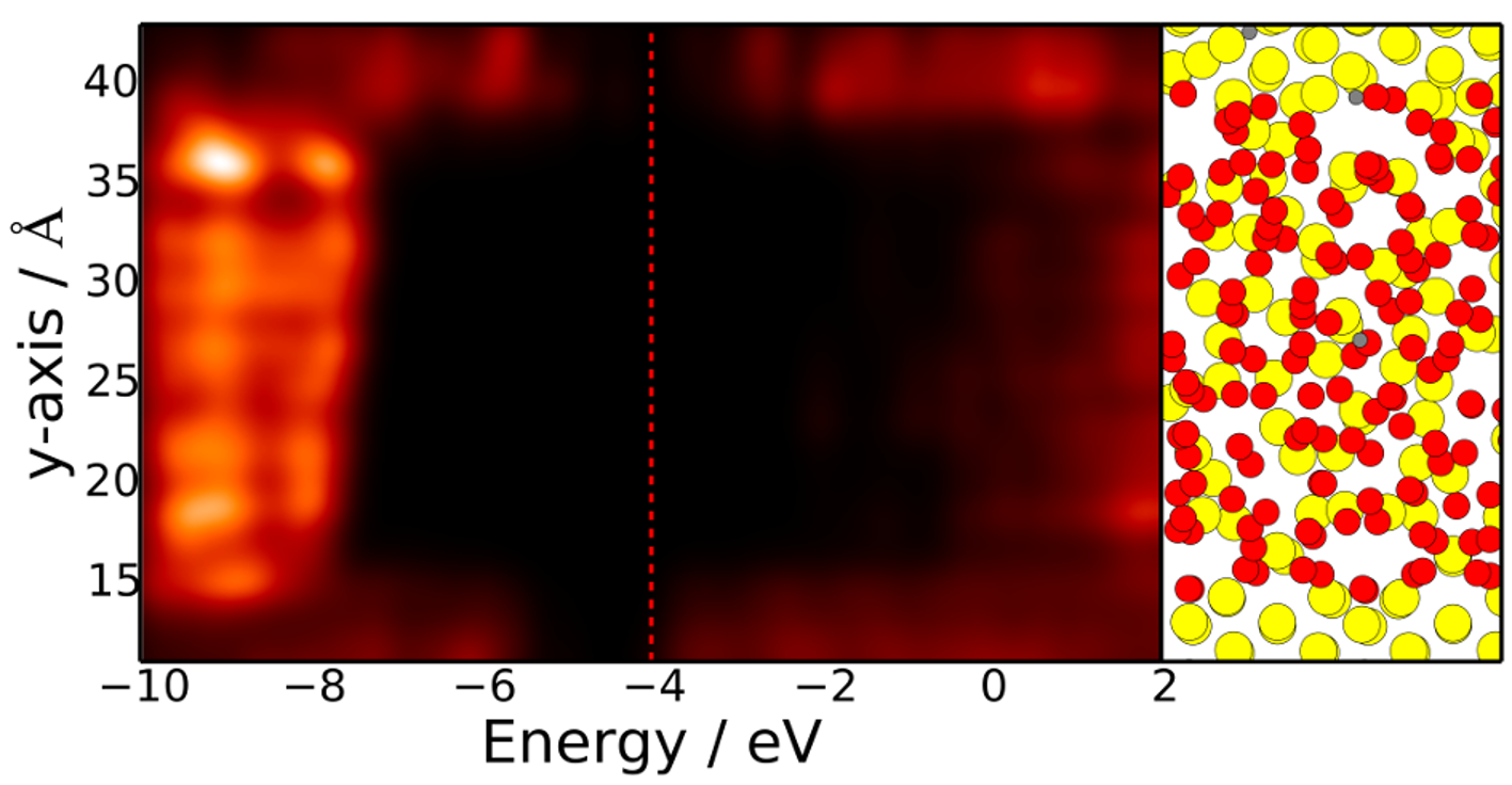
The calculation of defect properties in oxides is generally made under zero field conditions. The reliability issues mentioned above, however, occur under conditions of high electric field. We are currently assessing different methods of including an electric field in atomistic DFT calculations. We will then use these methods to understand how the properties of the defects change in response to an applied electric field in both amorphous silicon dioxide and in models of the Si/SiO2 interface.

Fig. 1: Densities of state across an Si/SiO2 interface with 10 MV/cm applied across it. The Si band gap of 1.1 eV is clearly seen as the black section at the bottom of the figure. The SiO2 band gap of 8.9 eV can be seen in the middle of the figure. Band bending can be seen across the whole stack.


