 |
|
Biography
Lado Filipovic was born in Sarajevo, Yugoslavia in 1983. He studied electrical engineering at Carleton University, in Ottawa, Canada, where he received the degree of Bachelor in Electrical Engineering (2006) and Master in Applied Science (2009). He joined the Institute for Microelectronics in January 2010, where he completed his doctoral degree in December 2012. His scientific interest is focused on topography simulations of novel semiconductor processes and the effects of process variability on semiconductor geometries.
Impact of Fabrication on the Electrical Performance of Through Silicon Vias
Recently, the semiconductor industry has directed considerable effort towards introducing more functionality to applications beyond memory and logic through vertical, or three-dimensional (3D), integration. This involves the fabrication of electrical interconnections through the entire thickness of the wafer. At the core of vertical integration is a through-silicon via (TSV) which electrically connects the front and back sides of the wafer.
The processing steps to manufacture an open TSV include deep reactive ion etching (DRIE) followed by the deposition of an isolation oxide, a barrier layer, a metal film, and a passivation layer. The process is complex and some deviations in the process conditions are expected. An analysis is performed to correlate the variability sources on the equipment level to the electrical performance of the final device. Hence, the simulation flow properly accounts for the concentration of gases in the chamber during plasma deposition/etching, the wafer etching process itself, and the electrical parameter extraction.
It is not feasible to treat all three steps together in a unique physics-based model, but a more suitable approach is to resolve them separately, linking them in a forward chain. Despite a rigorous control of the injected species in the plasma chamber, some variation can be observed in the concentrations of relevant gases and the duration of their presence in the chamber. DRIE involves an initial polymer deposition step, followed by one or two etch steps for a two-step or a three-step cycle, respectively.
Due to the numerous steps used for TSV fabrication, there are several potential variation sources which must be considered. During the polymer deposition, C4F8 is injected into the chamber and some variation in the gas flow rate, and thus in the deposition-relevant CFx and ion fluxes, is noted. For the two-step cycles, the etch step is performed by the injection of SF6 into the chamber. Variation in the SF6 concentration results in a variation of the flux of the relevant F and ion etching species.
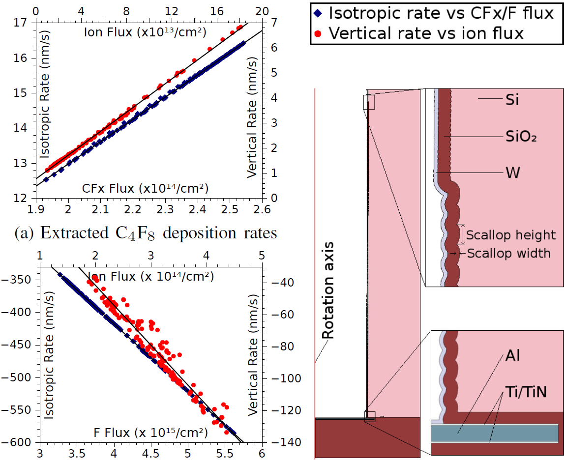
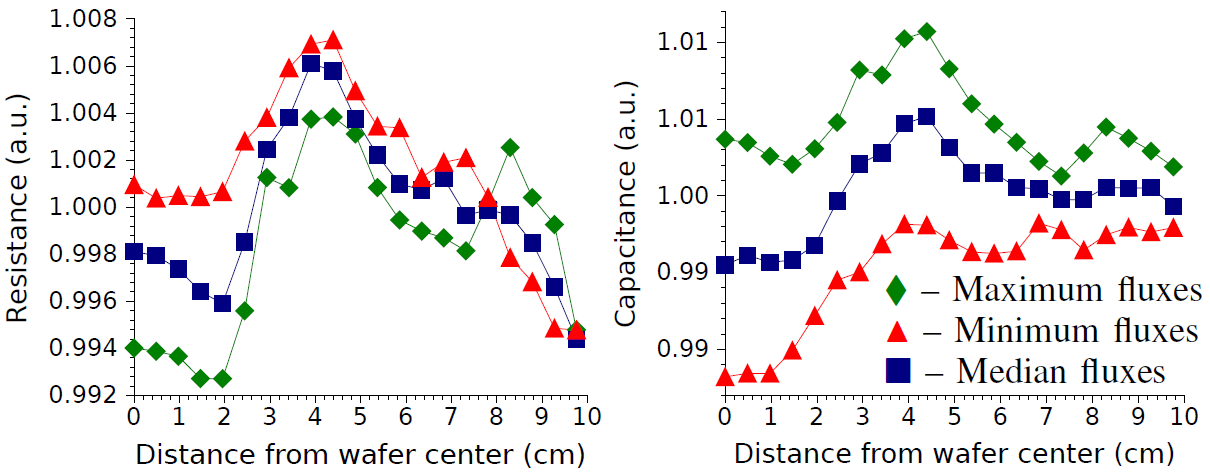
For the three-step DRIE processes, after the initial C4F8 polymer deposition, a SF6/O2 etch step is performed. This introduces an additional O flux which varies along with the gas concentration variation and plays a significant role in the silicon etching process. The effect of the neutral and ion fluxes on the isotropic and vertical deposition and etch rates are shown in Fig. 1, where a sample TSV geometry is also depicted. After applying the across-wafer variation of the relevant DRIE fluxes, the resulting across-wafer maximum, minimum, and median TSV resistance and capacitance have been extracted, as shown in Fig. 2. Although the individual fluxes can vary by up to 50% from the wafer center to the edge, the resulting resistance and capacitance variations remains within 1%.

Fig. 1: Extracted isotropic and vertical rates’ dependence on the neutral and ion fluxes at the wafer surface for the (left) polymer deposition and etching steps, and (right) a sample TSV geometry, prepared for electrical simulations. The fluxes shown are normalized from measurements to standard expected values.

Fig. 2: Across-wafer variation of the TSV electrical parameters. The values are calculated while applying the maximum, minimum, and median measured fluxes along the length of the wafer.


