 |
|
Biography
Yury Illarionov was born in Leningrad (now Saint-Petersburg) in 1988. He studied solid state physics at the Physical Science and Technology Faculty of St. Petersburg State Polytechnical University where he received the B.Sc. and M.Sc. degrees in 2009 and 2011, respectively. From 2010 to 2012 he studied advanced material science in Grenoble Institute of Technology (France) and University of Augsburg (Germany) in frameworks of Functionalized Advanced Materials and Engineering (FAME) Erasmus Mundus program and in September 2012 received a double European M.Sc. degree. His scientific carrier has started in October 2007 in Ioffe Physical-Technical Institute (Russia) and in November 2011 he joined the PhD program there. He also visited IRCELYON (France, May-July 2011) and Singapore Institute of Manufacturing Technology (Singapore, February-July 2012) as a young guest researcher. He joined the Institute for Microelectronics in February 2013. In January 2015 he received the PhD degree in semiconductor physics from Ioffe Physical-Technical Institute and in December 2015 the Dr.techn. degree from Technische Universität Wien. Since January 2016 Dr. Yury Illarionov is a postdoc researcher working on reliability of the next-generation 2D FETs with graphene, MoS2 and phosphorene.
A Systematic Study of Hysteresis in MoS2 Field-Effect Transistors
Molybdenum disulfide (MoS2) is a next-generation “beyond graphene” material which is now considered a promising candidate for future device applications. Already, MoS2 FETs have been successfully fabricated by different research groups. The characterization of their reliability is therefore becoming of great importance. For these new technologies the reliability study has to be started from the investigation of the device stability, which can be reduced by a considerable amount of fast oxide traps.
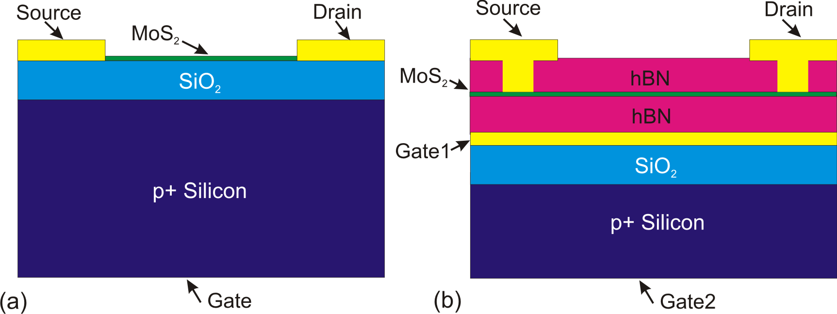
Most of the previous studies, however, have been restricted to statements confirming the existence of a hysteresis in the gate transfer characteristics for different measurement conditions. We have performed a systematic study of the hysteresis in our MoS2 FETs with SiO2 and hBN insulators (Fig. 1) by measuring the gate transfer characteristics using different gate bias sweep rates and sweep ranges. We found that the hysteresis widths extracted around the threshold voltage form a universal dependence versus the measurement frequency.
Analysis of these dependences for MoS2 FETs with different gate insulators (Fig. 2) shows that the hysteresis in MoS2/SiO2 FETs (Fig. 2(a)) is dominated by slower traps (f < 0.01Hz), while for MoS2/hBN/SiO2 devices (Fig. 2 (b)) moderately fast traps (0.01Hz < f < 1Hz) come into play. Furthermore, for MoS2/hBN FETs (Fig. 2(c)) the hysteresis is purely due to ultra-fast traps (f > 1Hz).
At the same time, in all three devices the hysteresis becomes smaller for narrower gate voltage sweep ranges, since the number of oxide traps that are able to change their charge state is smaller. Also, at higher temperatures the obtained frequency dependences become shifted towards higher f, which is especially pronounced for MoS2/hBN/SiO2 devices (Fig. 2(b)).
As such, we conclude that the traps which contribute to the hysteresis in our MoS2 devices are thermally accelerated. Finally, the proposed experimental technique is suitable for a systematic benchmarking of the hysteresis behavior in next-generation 2D FETs in general.

Fig. 1: Schematic configurations of our MoS2/SiO2 (a) and MoS2/hBN (b) transistors. The insulator thickness of both SiO2 and hBN is around 90 nm. The device with hBN has two gate contacts, one through the highly doped Si substrate and the other through a Ti/Au pad, which is situated between the SiO2 and hBN layers. The drain and source contacts are made of Ti/Au.

Fig. 2: (a) The frequency dependence of the hysteresis width measured for MoS2/SiO2 FETs using the gate voltage sweep ranges -20...20 V (top) and -20...0 V (bottom). The three datasets correspond to the results obtained before, during, and after six days of baking at T = 85 °C. The hysteresis is dominated by slower traps, which become partially annealed during baking. (b) The same goes for MoS2/hBN/SiO2 FETs measured using the sweep ranges −4…4 V (top) and 0…4 V (bottom). In both cases, we observe a maximum, which is reduced for narrower sweep ranges. At T = 85 °C the maximum is shifted towards higher f, which means that the time constants of the defects become smaller. (c) The corresponding results for MoS2/hBN FETs. Contrary to the previous two devices, the fraction of slower traps is negligible, while the hysteresis is dominated by ultra-fast traps.


