 |
|
Biography
Markus Kampl was born in Vienna, Austria, in 1988. He studied electrical engineering at the Technische Universität Wien, where he joined the Institute for Microelectronics in October 2012. In November 2015 he received the degree of Diplomingenieur. Since that time he is working on his doctoral degree.
Investigation of Hot Carrier Effects in Semiconductor Devices using Backward Monte Carlo
Accurate models of hot carrier effects in semiconductor devices are becoming more and more important. Methods used to calculate the high-energy tail of the distribution function, however, lack both the efficiency of classical Monte Carlo (MC) simulations and the accuracy of deterministic solvers. The backward MC (BMC) method is promising due to its accuracy, resulting from the use of the full-band structure, and its efficiency, arising from the use of a novel variance reduction technique.
The method was implemented in the simulator VMC (Vienna Monte Carlo). In classical MC simulations, huge simulation times were required to sufficiently reduce the variance of an estimator that depends on rare events only. The backward method, on the other hand, generates rare events directly and traces the phase space trajectories back in time until their injection points are reached. These backward trajectories allow for the calculation of the probabilities of rare events and thus of statistical averages in rarely visited phase space regions. In contrast to forward Monte Carlo algorithms, this method can easily calculate the high-energy tail of the carrier distribution function, which is necessary for a quantitative description of hot carrier effects.
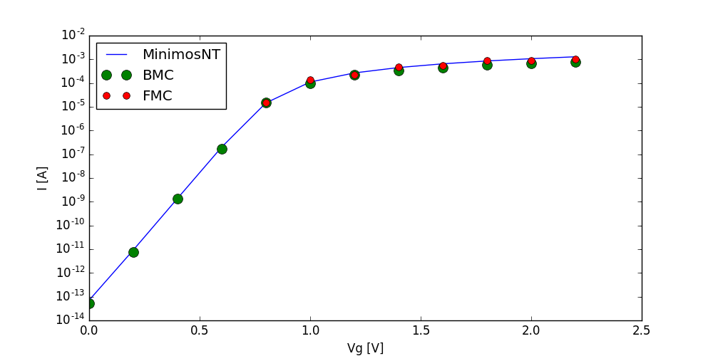
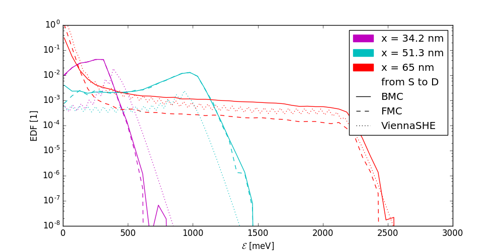
The I/V curve of an n-channel MOSFET was calculated using the drift diffusion simulator MinimosNT, the backward MC, and the classical MC methods. The advantage of the BMC method is that the trajectories begin at the energy barrier's maximum. Consequently, the current can be calculated over many orders of magnitude. Interestingly, the statistical error even decreases as the barrier increases. The high-energy tail of the distribution function was calculated using the BMC method and the deterministic spherical harmonics solver ViennaSHE. The results of the simulations are comparable over several orders of magnitude.

Fig. 1: Transfer characteristics of an nMOS device, simulated with MinimosNT, the FMC and BMC methods. Drain voltage is set to 2.2 V.

Fig. 2: Energy distribution function cuts through a 65 nm nMOS channel at V_GS = 2.2 V and V_DS = 2.2 V.


