 |
|
Biography
Hans Kosina received the Diplomingenieur degree in electrical engineering and PhD from the Technische Universität Wien in 1987 and 1992, respectively. He was with the Institute of Flexible Automation at the Technische Universität Wien for one year and then joined the Institute for Microelectronics, where he is currently an Associate Professor. He received the venia docendi in microelectronics in 1998. In the summer of 1993, he was a visiting scientist at Motorola Inc., Austin, Texas, and in the summer of 1999, a visiting scientist at Intel Corp., Santa Clara, California. Dr. Kosina served as a Technical Program Committee member in the IEEE International Workshop on Computational Electronics in 2003 and 2004 and was the chairman of the ''11th International Workshop on Computational Electronics'' held in Vienna in May 2006. He has served as the Associate Editor of the IEEE Transactions on Computer-Aided Design of Circuits and Systems since January 2004. His current research interests include the device modeling of semiconductor devices, nanoelectronic devices, organic semiconductors and optoelectronic devices, the development of novel Monte Carlo algorithms for classical and quantum transport problems, and computer-aided engineering in ULSI-technology.
Electronic Transport in Semiconductor Devices and Nanostructures
A new Monte Carlo (MC) algorithm for the solution of the semi-classical Boltzmann equation has been developed, which is especially suited to the calculation of the high-energy tail of the carrier distribution function. Accurate knowledge of the high-energy tail is a key ingredient to theoretically predicting hot carrier degradation effects. The theory of the so-called backward Monte Carlo (BMC) method was initially published in the 1980s. In 2003, a stability problem with the original method was discovered and a stable version was then proposed.
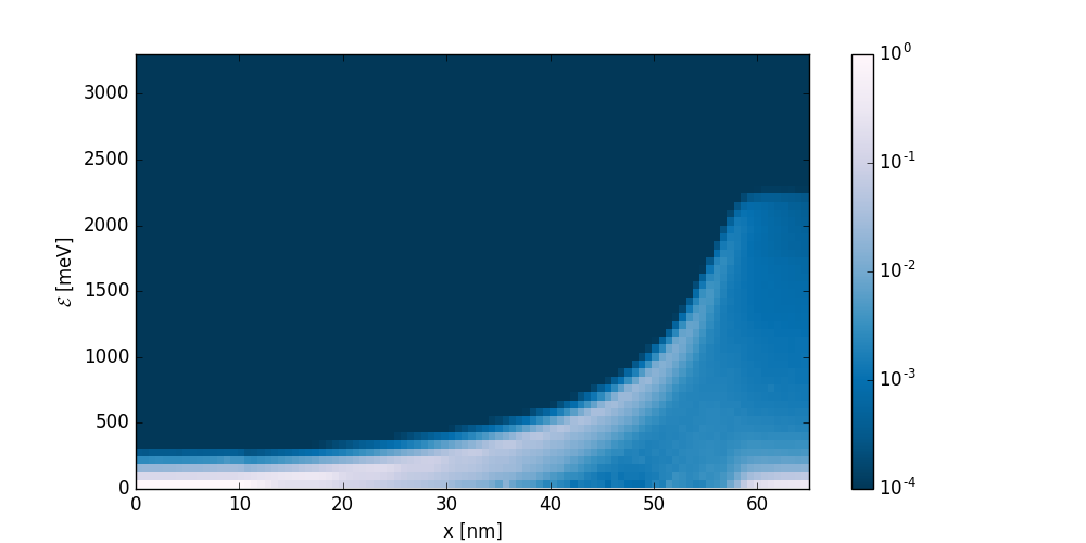
In our recent work, the BMC method has been augmented by various estimators required for device simulation, such as current estimators but also error estimators. The method has been implemented in the full-band Monte Carlo simulator VSP (Vienna Monte Carlo). In the BMC method, rare events of interest are generated directly, and the phase space trajectories, which lead to these events, are traced back in time until a contact is reached. There, the distribution function is prescribed as a boundary condition that allows the statistical weights of the backward trajectories to be determined. In this way, statistical averages in rarely visited phase space regions can be calculated. The VSP has been coupled with the classical device simulator MINIMOS-NT. The entire I/V characteristics of a MOSFET, including the sub-threshold region and the off-state, can now be studied by the full-band BMC method. The high-energy tail of the distribution function and the so-called acceleration integral, a quantity varying over more than twenty decades, can now be easily calculated using the BMC method.
We have also continued our theoretical studies on 2D materials. Transition metal dichalcogenides (TMDs) offer promising electrical, mechanical, and optical properties. We have performed a comprehensive analysis of the effect of strain on the mobility of MoS2, MoSe2, WS2, and WSe2, employing ab initio calculations of the band structure and the linearized Boltzmann equation for mobility evaluation. We included the effects of intrinsic phonons, remote phonons, and charged impurities. The lowest- and the second-lowest band minima in the conduction band of these materials are denoted as K- and Q-valleys.
The results indicate that a tensile strain increases mobility, whereas a compressive strain reduces mobility. Unstrained mobility and mobility enhancement with a strain are strongly dependent on the energy distance between the K- and Q-valleys. A small tensile strain has a higher impact on the mobility of materials with a smaller energy distance between the valleys, such as MoSe2 and WSe2. Our results indicated that monolayers of MoSe2 and WSe2 could serve as excellent base materials for highly sensitive strain gauges. Unlike conventional strain gauges, in these materials the inter-valley phonon-limited mobility is strongly affected by strain, which causes the large gauge factors.
Furthermore, research on nano-structured thermoelectrics has continued. Understanding transport in such nano-structures is a difficult task as carriers are far from thermodynamic equilibrium and quantum mechanical effects are dominant. Using the Non-Equilibrium Green's Function (NEGF) approach we have been studying both, strategies to improve ZT in materials through the introduction of nano-sized potential barriers, and the fragility of these enhancements in the face of the natural random imperfections that would be expected in any realistic structure. Our work has highlighted both the potential for thermoelectric enhancement in low-dimensional super-lattice structures but also identified some of the key culprits that can destroy this enhancement in real experiments.

Fig. 1: Electron energy distribution function in a 65 nm MOSFET obtained by a full-band backward Monte Carlo simulation.


