 |
|
Biography
Santo Papaleo was born in Novara, Italy, in 1988. He received the bachelor's degree in material science at the Università degli Studi del Piemonte-Orientale, and he received the master's degree in material science at the Università degli Studi di Milano-Bicocca in 2013. He joined the Institute for Microelectronics in 2013, where he is currently working on his doctoral degree. His scientific interests include stress estimation in TSV.
Mechanical Effects of the Deposition Process on TSV Sidewalls
Three-dimensional (3D) technology is essential in order to maintain integrated circuit performance along the path described by Moore's law. In this context, through silicon via (TSV) interconnects are used, and by necessity, they have complex architectures, consist of different materials, and include some geometric features of small size. Open TSV technology has been introduced in order to decrease failure due to thermomechanical effects.
A typical characteristic of the open TSV structures used in our studies is their employment of tungsten as a metal layer. Due to deposition and thermal processes, tungsten exhibits a high level of intrinsic tensile stress. The mechanical stress in the conductor line is usually in the GPa range. This may lead to delamination, cracking, voiding, and ultimately line failure. The study of interconnect mechanical reliability has, therefore, an important role to play. In particular, an understanding of the origin and development of mechanical stress within the thin film is crucial.
By considering polycrystalline metal films deposited onto polycrystalline or amorphous substrates, it has been observed that the Volmer-Weber mode is the main growth mechanism. Two different deposition processes due to different material properties are available during Volmer-Weber growth. If the deposited metal has a high melting point (Cr, Fe, Ti, W), the deposition process will exhibit low-mobility Volmer-Weber growth. On the other hand, high-mobility Volmer-Weber growth takes place when the metal deposited has a low melting point (Ag, Cu, Au).
In our work, we consider Volmer-Weber growth for tungsten and copper materials. Our studies focus on the sidewall interconnection area of open TSV structures. By using COMSOL Multiphysics, finite element method (FEM) simulations are employed to reproduce the deposition process. Different boundary conditions, as well as geometric parameters, are used in order to analyze how stress evolves during the growth process.
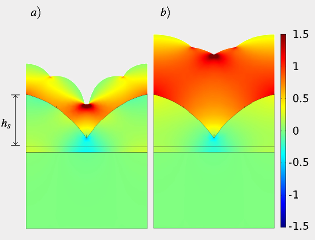
Due to the etching process, which is part of the production process of open TSVs, the formation of local geometric features, termed scallops, along the sidewall has been observed. The presence of a scalloped sidewall influences the stress distribution in the tungsten layer. The final stress distribution is a function of the tungsten layer's thickness (see Fig. 1). In our simulations, we have reproduced the film growth process on a scalloped structure, demonstrating a significant decrease in film stress compared to full plate samples without scallops. Our approach to these simulations can be considered an important tool for optimizing the design of TSV structures and can better provide an understanding of the development of mechanical stress.

Fig. 1: Components of the stress tensor σxx (in GPa) within the scallop structures for two different tungsten film thicknesses: a) 200nm, b) 400nm.


