 |
|
Biography
Marco Rovitto was born in Milan, Italy, in 1985. He studied material science at the Università degli Studi di Milano-Bicocca, where he received the bachelor's degree in 2010 and the master's degree in 2013. He joined the Institute for Microelectronics in January 2014, where he is currently working on his doctoral degree. His scientific interests include electromigration, interconnects, and process simulations.
Electromigration Induced Voiding and Resistance Change in Open Through Silicon Vias
Open through silicon vias (TSVs) are direct electrical connections from the top to the bottom of a silicon wafer of a chip that provide higher performances per unit area in three-dimensional (3D) integrated circuits. Although open TSVs show clear advantages, and the TSV process has almost reached the status of being a legitimate industry manufacturing technique, reliability concerns may always occur in such new, emerging technologies.
Electromigration (EM) is one of the key reliability issues in TSV structures, which is a wear-out failure mechanism caused by material transport due to current flow in metal lines. Typically, the EM wear-out mechanism is characterized by the nucleation of voids that grow and trigger chip failure. In TSV technologies, geometric features and material properties of the diverse metallic layers can lead to EM-induced voiding under the TSV. Voids nucleate especially at those locations in the structure where the adhesion between the metal line and the surrounding layer is weak. Consequently, void nucleation interfaces are a key aspect of the interconnect failure mechanism.
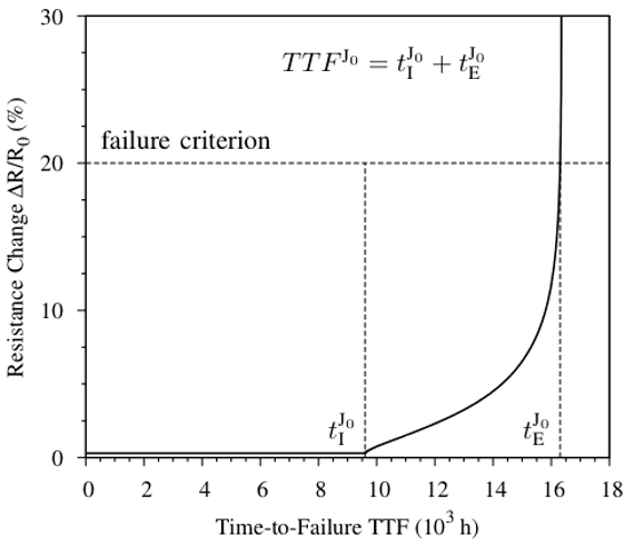
EM failure development is normally described by the interconnect's resistance change in time. Interconnect resistance as a function of time is typically divided into two parts. The first part, namely the void initiation phase, is characterized by the nucleation of a void that remains electrically undetectable. Interconnect resistance therefore remains constant during the entirety of the void-initiation period. The nucleation of a void marks the beginning of the second part, which is referred to as the void evolution phase. During this phase, the void evolution mechanism leads to a rapid non-linear interconnect resistance increase. The interconnect fails after a maximum tolerable resistance level is reached. Time-to-failure (TTF) is defined as the time needed to achieve this maximum resistance value. Consequently, predicting the EM TTF becomes crucial for the assessment of interconnect reliability.
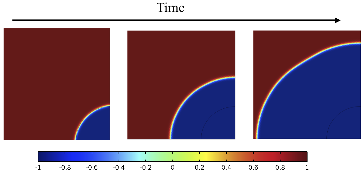
A two-step approach, based on the full EM model, is typically followed in order to determine the resistance change due to EM-induced voiding in open copper TSVs and to estimate the EM lifetime of a given interconnect. First, the locations with the highest probability of void nucleation are identified by monitoring the build-up of stress due to EM within the TSV structure. The EM void initiation time (tI) is defined as the time necessary to reach the threshold stress value for void nucleation. The second step is then characterized by the void evolution. An initial small void is placed at the void nucleation site, and its evolution is traced, including the increase of resistance, by using the phase field model (Fig. 1).
An analytic model based on the void radius dependence of the incoming vacancy flux due to EM is proposed to describe the time needed to grow a void of a given volume. The interconnect's resistance changes in time until it reaches the common failure criterion of 20% resistance increase (Fig. 2). The EM void evolution time (tE) is related to the time elapsed until this value is achieved. The EM TTF of the open TSV structure is given by the sum of both void initiation and void evolution times. This model, which combines the kinetics of void nucleation and growth, provides a good basis for EM TTF estimation. It describes EM failure development under the influence of different operating conditions, geometric features, and material properties. In this way, the EM lifetime of different interconnects can be predicted, which is crucial for the assessment of interconnect reliability.

Fig. 1: Phase field variable distribution of the evolving void in the open TSV structure under electrical loading.

Fig. 2: EM resistance trace profile.


