 |
|
Biography
Bianka Ullmann was born in Sofia, Bulgaria, in 1984 and has been in living in Vienna since 1991. She received the degree of Diplomingeneur in physics from the Technische Universität Wien in 2012. She has been working as a project assistant at the Technische Universität Wien since 2013 and joined the Institute for Microelectronics in January 2014.
Thermally Activated Recovery of MOSFETs after BTI and HCD Stress
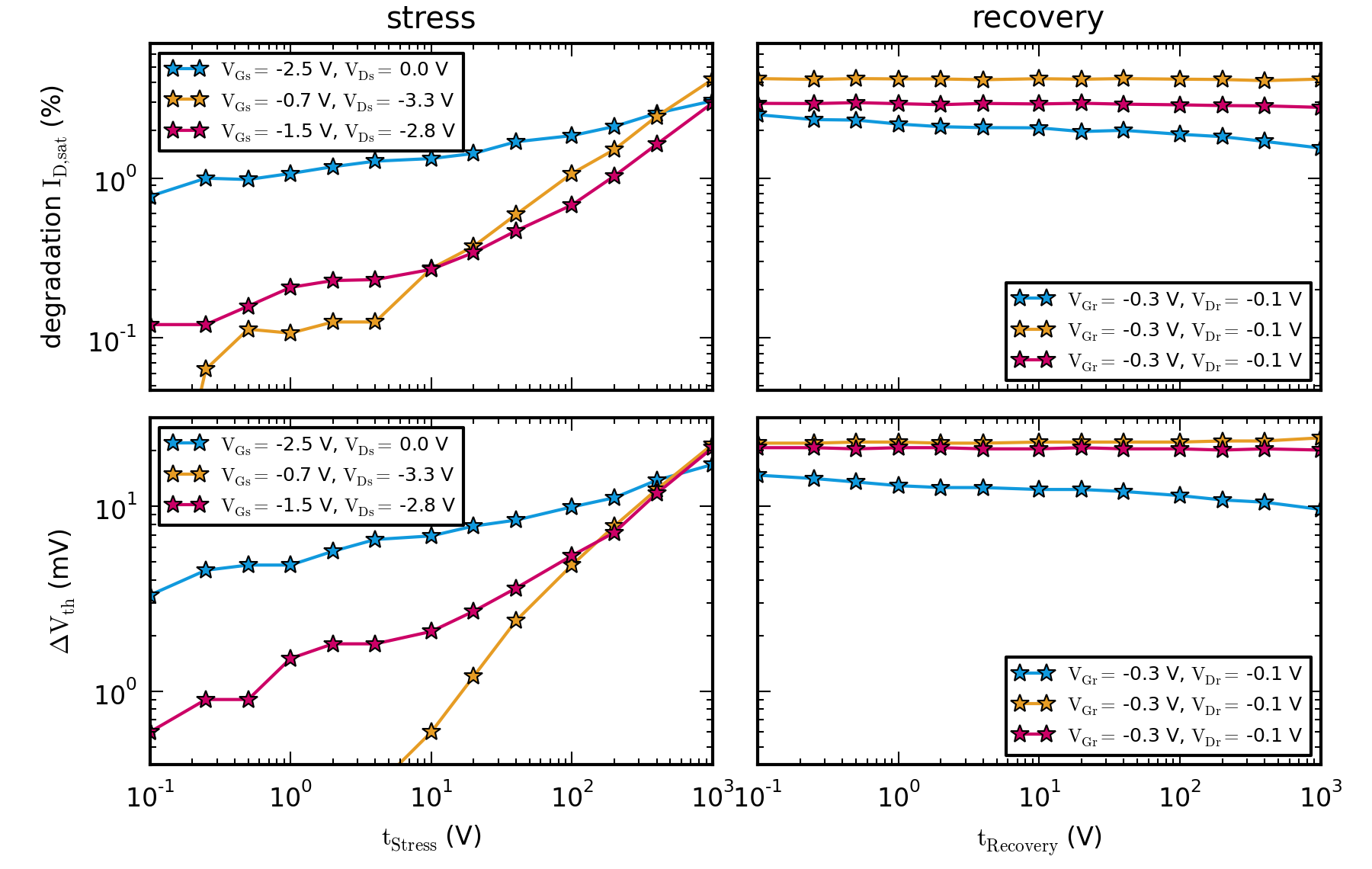
Degradation mechanisms of metal-oxide-semiconductor field-effect transistors (MOSFETs), such as bias temperature instability (BTI) and hot carrier degradation (HCD), are caused by material defects in the amorphous gate oxide. Defects can capture or emit charge carriers from the Si substrate and from the gate oxide. These capture-and-emission events cause a change in the current between gate and source at constant gate-source voltage and drain-source voltage. This electrical response corresponds to an unwanted change in device characteristics, as shown on the left-hand side of Fig. 1 for a pFET device. Measurements of this detrimental behavior allow us to characterize the impact of different stress conditions on device characteristics and in the case of nano-scale MOSFETs, to observe the nature of individual defects responsible for unwanted changes in device characteristics.
The typical capture-and-emission times of traps vary by many orders of magnitude, from µs to weeks, depending on their properties, the temperature, and the bias conditions applied to the MOSFET. Fig. 1 depicts the dependence of the degradation and recovery behavior of the drain current in saturation (IDsat) and the threshold voltage change (deltaVth) on the voltage stress conditions. The two subplots on the right-hand side reveal that damage caused by different stress conditions recovers in different ways and under some conditions, not at all within the measurement window. This seemingly permanent damage is caused by traps with very large emission times. By increasing the temperature, these emission events are shifted into experimentally feasible timeslots. In other words, the recovery process is accelerated.
In order to observe defects with a broad range of capture-and-emission times, we have developed a hardware and software application for temperature control of local polysilicon heater structures within the time-dependent defect spectroscopy (TDDS) framework. We are able to apply controlled temperature pulses during device recovery within the TDDS sequences. This will allow us to characterize the properties of a multitude of defects that cause seemingly permanent device degradation. From future measurements, we expect to make a significant contribution to the understanding of the nature of traps, the component of permanency, and the interaction between different degradation mechanisms.

Fig. 1: Behavior of two characteristic device parameters, IDsat and deltaVth, during stress and recovery.


