 |
|
Biography
Yannick Wimmer was born in Steyr, Austria, in 1985. He studied physics at the Technische Universität Wien, where he received the degree of Diplomingenieur in 2012. He joined the Institute for Microelectronics in August 2012, where he is currently working on his doctoral degree. His current scientific interests include channel hot-carrier effects and NBTI.
Non-Parabolic Potential Energy Surfaces of Oxide Defects
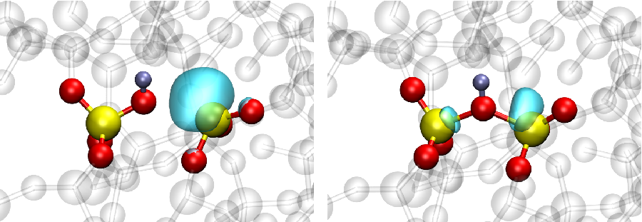
A potential energy surface (PES) describes the energy of a system with respect to certain parameters, normally the positions of the atoms. The most stable configuration of any system of atoms is always at the minimum of its PES. If a defect in silicon dioxide (SiO2) changes its charge state, the atomic configuration also changes to obtain the minimum of the new PES (see Fig. 1). These minima can be found using density functional theory (DFT) calculations. We are not only interested in the minimum energies, however, but especially in the transition barriers between different charge states. Conventionally, transitions between two charge states of a defect were assumed to be best modeled using harmonic oscillators and therefore a parabolic approximation of the PES. According to nonradiative multiphonon theory (in the classical limit) transitions occur at intersections of these PESs, determining the reaction barriers.
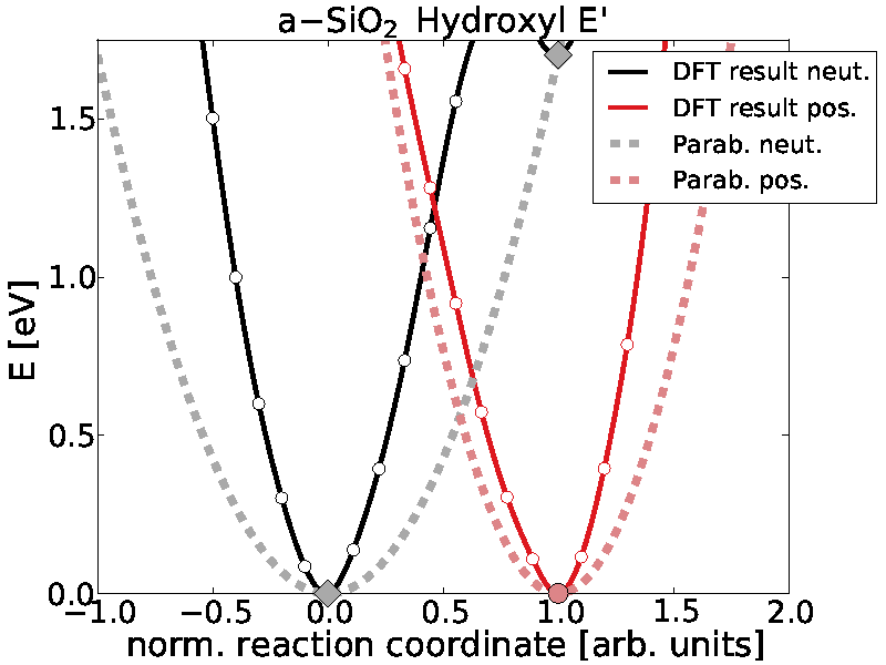
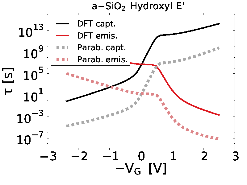
We investigated whether this parabolic approximation is justified. We therefore interpolated (and extrapolated) atomic configurations from the two minimum configurations and computed the PES along this direct reaction path using DFT calculations. As can be clearly seen in Fig. 2, these PESs differ considerably from the parabolic approximation. Even though the deviation is only in the range of tenths of electron volts, one must bear in mind that charge-capture and emission times depend exponentially on the reaction barrier. A reduction in the reaction barrier by a few percent can therefore lead to a reduction in the charge-capture and emission times by several orders of magnitude. Fig. 3 shows how such defects would behave in the gate oxide of a transistor at several gate voltages, i.e. at different electric field strengths in the oxide. The electric field shifts the parabolas relatively to each other along the y-axis in Fig. 2, thereby changing the reaction barrier.
We found that reaction barriers tend to be underestimated by a parabolic approximation for all hydrogen-related defects in SiO2. We can therefore conclude that capture and emission times also tend to be severely underestimated in models based on parabolic approximations of the PES.

Fig. 1: Hydroxyl-E' center defect in its neutral (left) and positive (right) charge state. H atoms are shown as silver, Si atoms as yellow and O atoms as red. The turquoise bubble represent the localized highest occupied orbitals for the neutral charge states and the lowest unoccupied orbital for the positive charge states.

Fig. 2: Comparison between a parabolic approximation of the PES (dashed lines) and the PES deduced from DFT results (solid lines) of a selected defect. The crossing point, which determines the reaction barrier, is severely underestimated by the approximation.

Fig. 3: Comparison between capture and emission times of a specific defect in the gate oxide of a transistor, calculated using a parabolic approximation of the PES (dashed lines) and the PES deduced from the DFT results of Fig. 2 (solid lines). Both capture and emission times are severely underestimated by the approximation.


