The first HEMTs were developed mostly for low noise applications like receivers [73, 74, 75]. The noise of an amplifier is characterized by the noise figure F which is defined as the signal-to-noise ratio at the amplifier output divided by the signal to noise ratio at the input. Noise figures of a two stage amplifier as low as 1.7 dB with an associated gain of 17 dB at 32 GHz were obtained [73].
The principal source of noise added by the transistor at high frequencies
are related to power dissipation in the resistances of the device. At lower
frequencies generation/recombination processes become dominant. General
dependencies of Fmin on device parameters can be obtained
from Fukui's equation [76].
Fukui showed that
 |
(61)
|
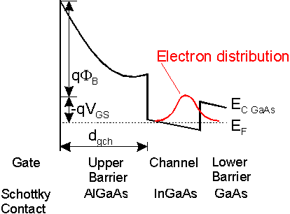
From a microscopic point of view important noise sources are scattering mechanisms such as alloy fluctuations and interface roughness on heterojunctions. These will have an impact on the device parameters such as resistances, thus they are indirectly included in (61). The conduction band diagram and the electron distribution at the low noise bias point, i. e. near VT, is shown schematically in Figure 6.5. As depicted in the diagram the maximum of the electron distribution is near the lower heterojunction interface of the channel. Therefore, this interface is considered to be very important.
During the growing sequence of a typically pseudomorphic HEMT the surface
morphology of AlGaAs is inferior to pure GaAs which increases the roughness
of the heterojunction interface and thus the electron scattering. To reduce
scattering and thus noise, pure GaAs is used below the channel. Such HEMTs
without an AlGaAs barrier below the channel are referred to as single heterojunction
HEMTs (SHHEMTs).

Besides Fmin good RF performance of low noise HEMTs
is required. As discussed in Section 5.2 the transconductance
gm near VT is not simulated very well,
thus the determination of Fmin using (61)
by simulation will not be further investigated directly. But (61)
reveals that a large ratio gm/CGS is necessary
for a low Fmin which are similar requirements as for
high fT . It can be expected that devices with a high
maximum fT will also exhibit low Fmin.
Therefore, low noise HEMTs will be investigated with respect to their RF
performance at VDS = 2.0 V and gm max.
Helmut Brech 1998-03-11