Applying the method of Bernoulli [103], the homogenous part
of (4.13) is expressed by
 with with |
(7.1) |
which enables separation to
 and and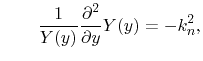 |
(7.2) |
with
 and and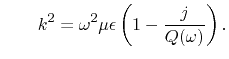 |
(7.3) |
The general solution of these equations is
 and and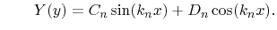 |
(7.4) |
The PMC boundary (4.16) on the open slot and the PEC
boundaries (4.15) on the metallic walls according to
Figure 7.1 are introduced by
![\begin{displaymath}\begin{array}[t]{ccc}
&&\\
X(0)=X(L)=0&\Rightarrow&B_{m}=0...
...}}\quad\forall\quad
n\in\mathbb{N}_{0}.\\
&&\\
\end{array}\end{displaymath}](img471.png) |
(7.5) |
 and
and  are the eigenvalues of (4.13) for the
rectangular enclosure in Figure 7.1. The fringing fields at the
slot are considered by using the effective enclosure width
are the eigenvalues of (4.13) for the
rectangular enclosure in Figure 7.1. The fringing fields at the
slot are considered by using the effective enclosure width
 instead of
  .
In [45]
.
In [45]
 has been taken to consider the fringing fields for
planes with two open boundaries associated with dimension , but as the enclosure in
Figure 7.1 has only one open edge, the correction must be
performed by using
. An additional correction has to be carried out to
consider the wall thickness
has been taken to consider the fringing fields for
planes with two open boundaries associated with dimension , but as the enclosure in
Figure 7.1 has only one open edge, the correction must be
performed by using
. An additional correction has to be carried out to
consider the wall thickness  of the enclosure. This is not necessary in the case
of power planes on a PCB, because the conducting layers are thin, although, a metallic
enclosure usually has thicker walls. To consider a non-negligible wall thickness of the
enclosure, the effective enclosure dimension in y-direction is
of the enclosure. This is not necessary in the case
of power planes on a PCB, because the conducting layers are thin, although, a metallic
enclosure usually has thicker walls. To consider a non-negligible wall thickness of the
enclosure, the effective enclosure dimension in y-direction is
 |
(7.6) |
With (7.5) and (7.4) the solution
of the homogenous part of (4.13) results in
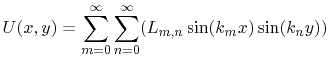 |
(7.7) |
 are parameters which depend on the integer pair
  and
and  . These parameters
are obtained by the following solution of (4.13).
The port excitation with a current
. These parameters
are obtained by the following solution of (4.13).
The port excitation with a current  on source point
 is
expressed by
is
expressed by
 |
(7.8) |
where
 is the Dirac impulse. Consistency with standard voltage and
current direction of the impedance matrix (4.17) is achieved with
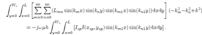
the negative sign. Inserting (7.7)
and (7.8) into (4.13), multiplying with
is the Dirac impulse. Consistency with standard voltage and
current direction of the impedance matrix (4.17) is achieved with
the negative sign. Inserting (7.7)
and (7.8) into (4.13), multiplying with
 and integrating over the area
 yields
 |
(7.9) |
Where
 and
and
 . The right hand side
of (7.9) becomes
. The right hand side
of (7.9) becomes
 |
(7.10) |
The left hand side of (7.9) vanishes for all  and also for
all
and also for
all  according to the orthogonality of the base functions
 to
to
 and
and
 to
to
 , respectively. For
  and
and
 the left hand side integral solutions are
![$\displaystyle \int_{x=0}^{L}\left[\sin^2(\frac{m\pi x}{L})\textrm{d}x\right]=\frac{L}{2},$](img495.png) |
(7.11) |
and
![$\displaystyle \int_{x=0}^{W_{e}}\left[\sin^2(\frac{(2n+1)\pi
x}{2W})\textrm{d}y\right]=\frac{W_{e}}{2}.$](img496.png) |
(7.12) |
Finally, the solution of (4.13) for the rectangular enclosure in
Figure 7.1 becomes
![$\displaystyle U(x,y)=\frac{j4\omega\mu hI_{sp}}{LW_{e}}\sum_{m=0}^{\infty}\sum_...
...}x_{sp})\sin(k_{n}y_{sp})\sin(k_{m}x)\sin(k_{n}y)}{k_{m}^2+k_{n}^2-k^2}\right].$](img497.png) |
(7.13) |
With (7.13) the coefficients of the impedance
matrix (4.17) are
![$\displaystyle Z_{ij}=\frac{j4\omega\mu h}{LW_{e}}\sum_{m=0}^{\infty}\sum_{n=0}^...
...)\sin(k_{n}y_{i})\sin(k_{m}x_{j})\sin(k_{n}y_{j})}{k_{m}^2+k_{n}^2-k^2}\right].$](img498.png) |
(7.14) |
The resonance frequencies of the enclosure obtained from the zeros of
 are
are
 |
(7.15) |
where
 denotes the speed of light in the cavity.
C. Poschalko: The Simulation of Emission from Printed Circuit Boards under a Metallic Cover