 |
|
||||
BiographyHajdin Ceric was born in Sarajevo, Bosnia and Herzegovina, in 1970. He studied electrical engineering at the Electrotechnical Faculty of the University of Sarajevo and the Technische Universität Wien, where he received the degree of Diplomingenieur in 2000. In 2005 he received his PhD in technical sciences and in 2015 his venia docendi (habilitation) in microelectronics from the Technische Universität Wien. He is currently an Associate Professor at the Institute for Microelectronics. His research interests include finite element method modeling and simulation in microelectronics, application of machine learning in computer numerics, atomistic modeling in material science, electromigration in metals, and mechanical reliability of metals and semiconductors. In 2010 he was appointed the head of the Christian Doppler Laboratory for Reliability Issues in Microelectronics with two participating industrial partners: ams AG and Infineon Technologies Austria AG. Dr. Ceric participated in several European Community and FFG projects. In his research, Dr. Ceric has been closely cooperating with a company SOITEC, France, and research center imec, Belgium. He is a reviewer for several American Institute of Physics, Elsevier, and IEEE journals. Research Topics:Interconnect Reliability |
|||||
Electromigration-Induced Growth of Silicon Nanowires
In recent years, it has been shown that electromigration can be utilized to change surface morphologies. The motion and shape transformation of multiple nanosized objects can largely be controlled during electromigration. One of the potential applications of this observed phenomenon is the fabrication of silicon nanowires. Silicon nanowires are typically grown vertically, directly from the silicon substrate. In addition, they must subsequently be cut and horizontally placed on a substrate, if they are to be integrated into planar devices. Alternatively, it has been proposed to grow silicon nanowires horizontally on top of silicon surfaces, which is a significant simplification compared to the vertical growth process.
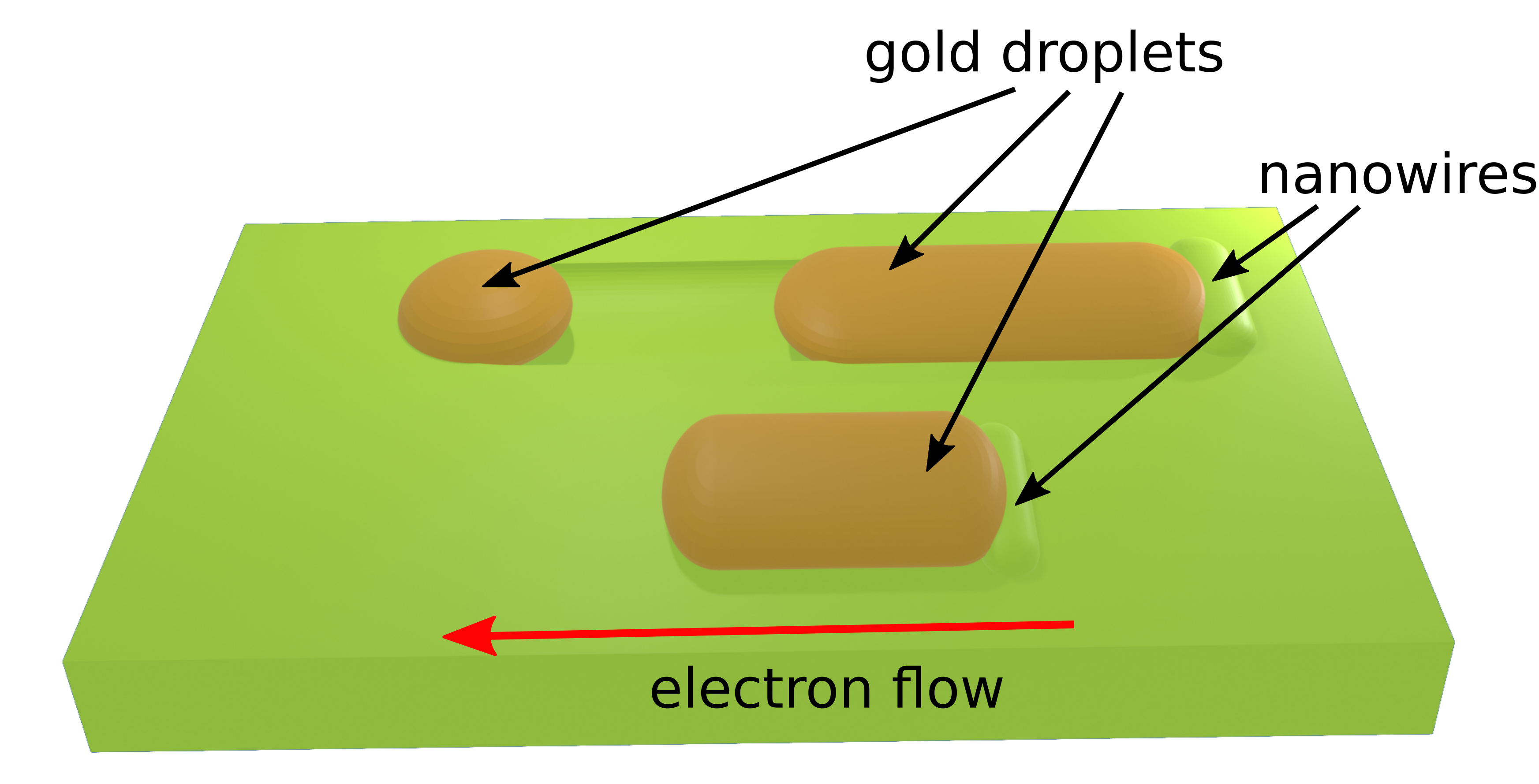
During the deposition of gold on a silicon substrate at temperatures above the eutectic point, which is the lowest temperature at which a mixture of two or more metals, or a metal and a non-metal, melts or solidifies, elongated liquid gold droplets move on top of the silicon substrate, driven by electromigration. A moving gold droplet leaves a formed in-plane silicon nanowire behind (see Fig. 1). If the droplets are not directed by electromigration, the randomness of their motion would limit the predictability of their final geometry, thereby limiting the perspective for their potential applications. We investigate the possibility of using electromigration-controlled gold droplets, deposited on a silicon substrate, to influence the growth of in-plane nanowires. We have developed a model which describes the change in a three-dimensional droplet surface under the impact of electromigration and droplet geometry.
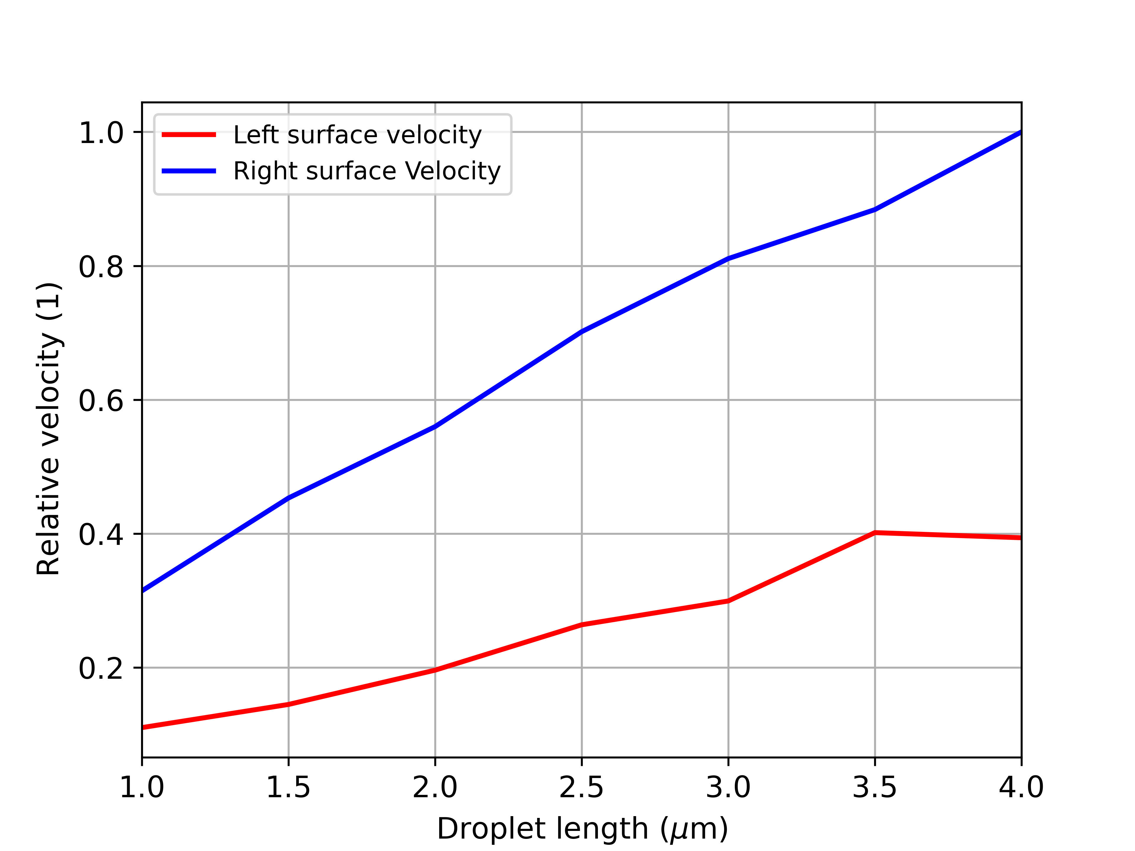
Experimental investigations on the formation of silicon nanowires have identified several partially overlapping phases during this process. These phases comprise gold droplet formation during deposition, dissolution of the silicon substrate beneath the droplet, transformation of the droplet shape governed by the minimization of the surface and interfacial energies, and migration and shape change under the influence of electromigration. Our model describes atomic transport at the droplet surface and inside the droplet. The redistribution of atoms causes a change in the droplet shape and position. From the atomic concentration, obtained by solving equations of atomic transport, we can deduce the normal velocity of the droplet surface at each point of the surface. Our simulations show that a droplet increases its length while migrating in the direction opposite to the current flow and that the dynamics of the droplet transformation is increased for longer droplets (see Fig. 2), which has previously been observed in experiments.

Fig. 1: Electromigration-driven movement of the gold droplets on top of the silicon substrate. The droplets leave silicon nanowires in their trail.

Fig. 2: Variation of droplet surface velocities with respect to droplet length. All velocities are scaled to the maximum velocity.


