 |
|
||||
BiographyLukas Cvitkovich was born in 1992 in Eisenstadt, Austria. He received his Bachelor degree in Electrical Engineering and his Diplom-Ingenieur degree in Material Sciences from TU Wien, where he defended his Master Thesis in the Quantum Materials group of the Institute of Solid State Physics in 2019. During his studies, he also worked as a research assistant at the Institute of Sensor and Actuator Systems and at the Institute for Solid State Electronics at TU Wien. In May 2020 he joined the Institute for Microelectronics where he started his PhD studies, focusing on the ab initio simulation of oxide defects in semiconductor devices. |
|||||
Variability due to Interfacial Disorder in Si-based Spin Qubits
Silicon is a particularly attractive material to host semiconductor spin qubits for quantum computation because the fabrication processes are well established and the main isotope 28Si is free of nuclear spins which may interact with the carrier spin via hyperfine interactions. In a spin qubit, the spin carrier is spatially confined in a semiconducting material, forming a quantum dot. The confining interfaces to adjacent regions play a crucial role in this context because they induce further coupling to the charge carrier’s valley and spin degree of freedom, which are exploited to coherently drive spin transitions. In the most successful types of Si-based spin qubits, the spatial confinement is realized by interfaces to SiO2 or SiGe. However, these interfaces are intrinsically disordered on an atomic scale, yielding detrimental variabilities of essential parameters such as the energy level splitting at the valence or conduction band edges of the semiconductor. This ultimately results in quantum decoherence, since even basic operations such as spin rotations cannot be carried out precisely. Distinct correction of the parameters of each device could quickly become a bottleneck, especially for applications like quantum computation, in which thousands of spins need to be controlled individually. While experimental evidence for significant variability in Si spin qubits has been reported, a better theoretical understanding could provide valuable insights for improving the reproducibility of Si-based quantum devices.
We study the valley and spin splitting of electrons in the Si X valley, confined in explicit atomistic models of Si/SiO2 and Si/SiGe nanostructures. Valley splitting results from interference effects between the Si kz and k-z valley states at the interface, and spin splitting arises due to a relativistic interaction of the particle’s spin with its motion along the inhomogeneous potential at the interface. The splittings are obtained from density functional theory (DFT) calculations.
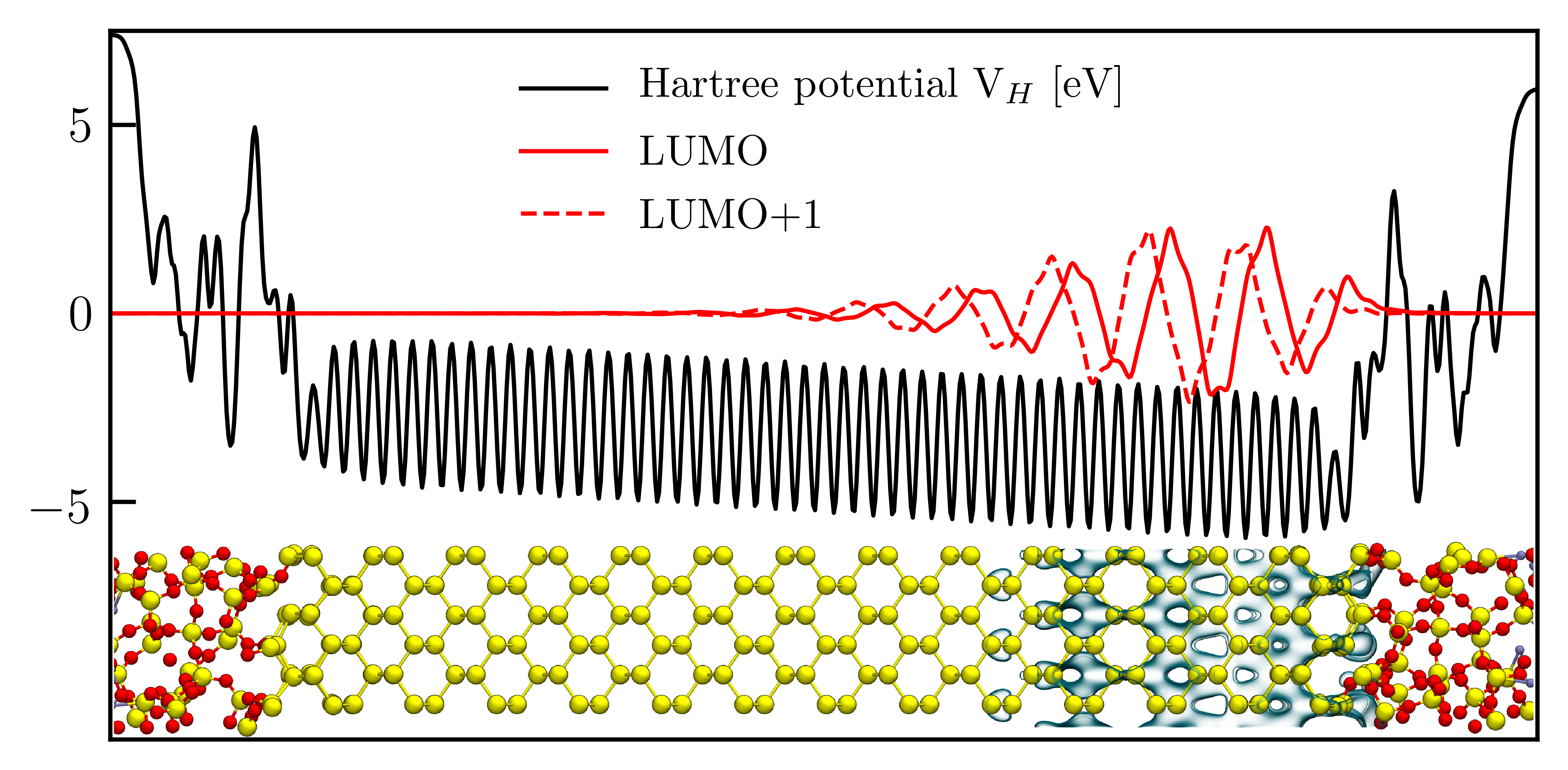
Due to the computational limitations of DFT - mesoscopic models of semiconductor spin qubit devices consist of millions of atoms - we investigate the influence of single interfaces only. Our realistic model structures consist of a Si slab (2 nm - 7 nm thick) confined by amorphous SiO2 or pseudomorphic SiGe in the (100) direction. The charge in the Si layer forms a two-dimensional electron gas (2DEG). By applying an electric field, we push the wavefunction against the Si/SiO2 or Si/SiGe interface, which decouples the wavefunction from the second interface. Additionally, the field breaks the time-reversal symmetry, allowing for spin-orbit coupling which splits the spin states in a valley in the presence of a magnetic field. Hence, we extract both valley and spin splitting due to confinement by a single interface. We explicitly compare similar disordered interfaces qualitatively and show that the resulting valley and spin splittings inherently vary within one order of magnitude, emphasizing the relevance of interfacial disorder for quantum devices.

Fig. 1: The wave functions of the 2DEG valley states are shown, averaged over the cross-section of the simulation cell. The states are confined in the Si quantum well by the oxide layers as represented by the Hartree potential from a DFT calculation. The two lowest conduction states lie in the kz and k-z valleys. The energy of the remaining four X valley states of Si increase as a result of the confinement along z. An electric field shifts the Hartree potential and pushes the wavefunction against the right interface, while decoupling it from the left one.


