 |
|
||||
BiographyLado Filipovic is an Associate Professor at TU Wien, working on Integrated Semiconductor Sensors and Process Simulation at TU Wien. He obtained his venia docendi (habilitation) in Semiconductor Based Integrated Sensors and his doctoral degree (Dr.techn.) in Microelectronics from TU Wien in 2020 and 2012, respectively. He holds a Master’s degree in Applied Sciences (MASc.) from Carleton University in Ottawa, Canada, which he obtained in 2009. He has been a Principal Investigator in various research projects funded by, e.g., the EU FP7 and Horizon 2020 programs, the Christian Doppler Forschungsgesellschaft, the Austrian Science Fund (FWF), and the Austrian Research Promotion Agency (FFG). He is a Senior Member of the IEEE and is an active member of the Technical Program Committee for outstanding IEEE sponsored conferences, such as IEEE Sensors, SISPAD, and IIRW. He has served as a reviewer for several funding agencies, has edited two books on Miniaturized Transistors, and is an active reviewer for many leading journals. Lado's primary research interest is studying the operation, stability, and reliability of novel semiconductor-based sensors using advanced process and device simulations. An additional pillar of his research is the multi-scale modeling of processes involved in the fabrication of semiconductor devices and sensors. This involves combining atomistic modeling with Monte Carlo and continuum approaches, as well as merging physical and empirical modeling in a single framework, specifically in process TCAD. He is also actively investigating metal oxide semiconductors and novel two-dimensional (2D) materials, e.g., graphene, MoS2, and phosphorene for the detection of biomarkers and environmental pollutants. In particular, his group is investigating the impact of the adsorption of ambient gas molecules on the surfaces of 2D semiconducting films and on the performance of devices and sensors based on these. Software Development:Process Simulator ViennaPS Research Topics:Semiconductor Sensors Running Public Projects:FWF - Adsorbate-Dependent Conductivity of MoS2 FETs CDG - CDL for Multi-Scale Process Modeling of Semiconductor Devices and Sensors FETs |
|||||
Physics-Informed Compact Modeling for Design-Technology Co-Optimization
Technology computer-aided design (TCAD) is an essential tool for the development and optimization of micro- and nanoelectronic devices and circuits. Especially when it comes to the integration of novel materials and fabrication processes, the use of TCAD in a design-technology co-optimization (DTCO) cycle has become indispensable. To enhance the performance of semiconductor-based devices and circuits, designers need to understand how even a single step in the fabrication process affects the semiconductor device geometry and the integrated circuit's operation, reliability, and variability. This understanding enables the circuit designer to give feedback to the fabrications engineer, who can modify the process to improve circuit performance. However, relying solely on experiments to establish this feedback loop involves extreme time and cost considerations. Hence, it is critical to integrate process simulations with device and circuit simulations through DTCO to design and optimize future semiconductor devices and technologies.
A critical problem with a DTCO implementation from fabrication to circuit is that the generation of process-aware geometries using physical modeling techniques typically requires stochastic processes and is very time intensive. The inclusion of equipment parameters in the simulation adds further complexity since equipment-level and wafer-level simulations require drastically different size scales. Therefore, there is a need to provide geometries which capture the relevant equipment settings in a fast way for DTCO. For this, we have implemented a workflow which links equipment parameters and physical processes together in order to collect sufficient data to train compact models. These compact models are then applied to generate process-aware geometric structures quickly and efficiently, which can easily be integrated in a TCAD flow to inform on the process' impact on device and circuit designs.
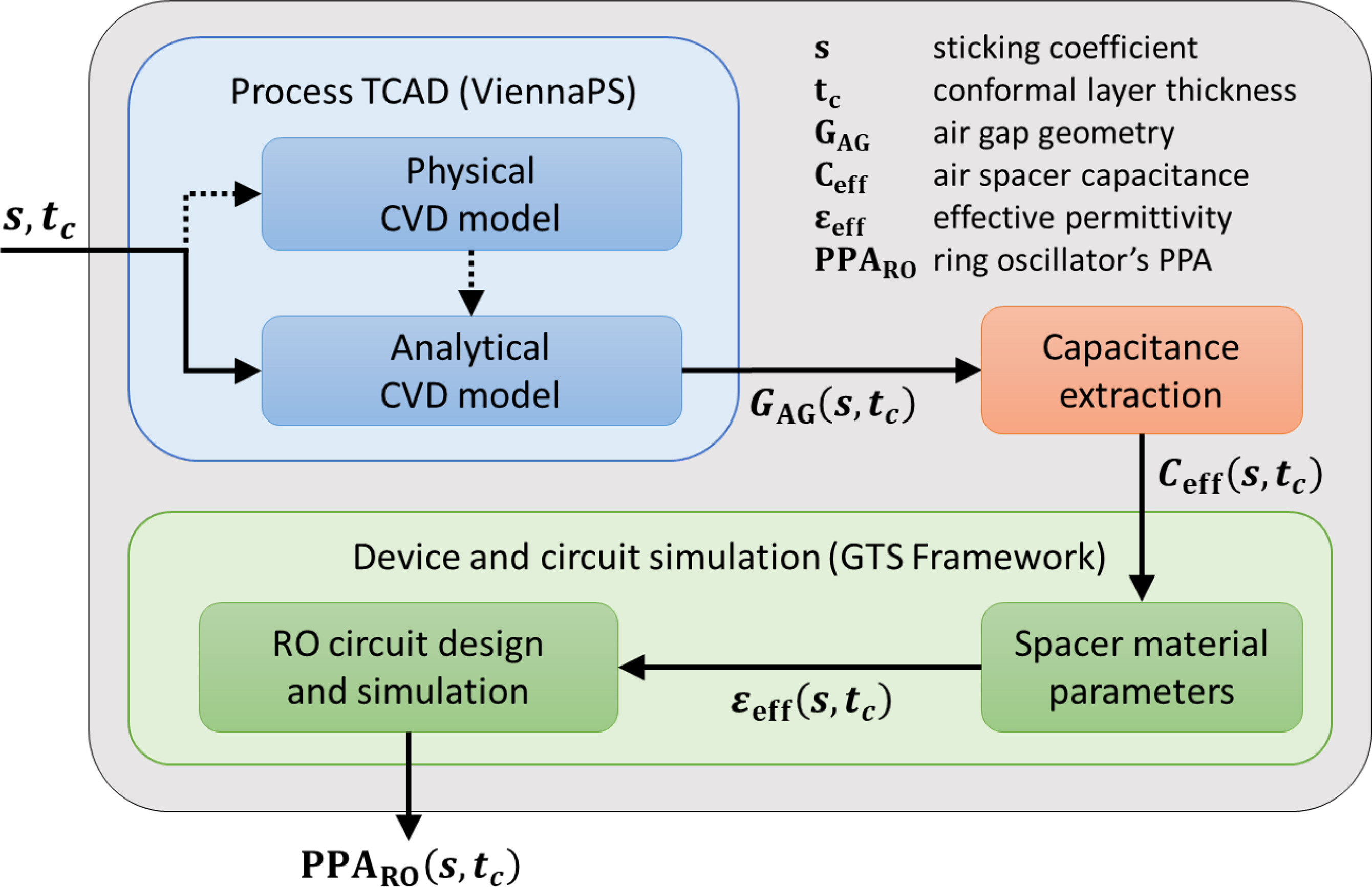
We have implemented a compact model for chemical vapor deposition (CVD) in a trench for the purpose of air spacer generation at the 7 nm technology node. This model was then integrated in a DTCO flow to extract the impact of the parameters which form the spacer on the power and performance of a 5-stage ring oscillator. The air spacer is usually filled by sequential conformal and non-conformal silicon nitride deposition steps. The impact of the thickness of the conformal layer and the sticking probability during non-conformal deposition on the effective spacer permittivity and capacitance was studied by solving the Poisson equation on the final geometry. Ultimately, SPICE model cards were extracted from the TCAD characteristics to form a parasitics network for the full three-dimensional (3D) ring oscillator logic cell using a field solver. The full DTCO sequence is provided in Fig. 1.
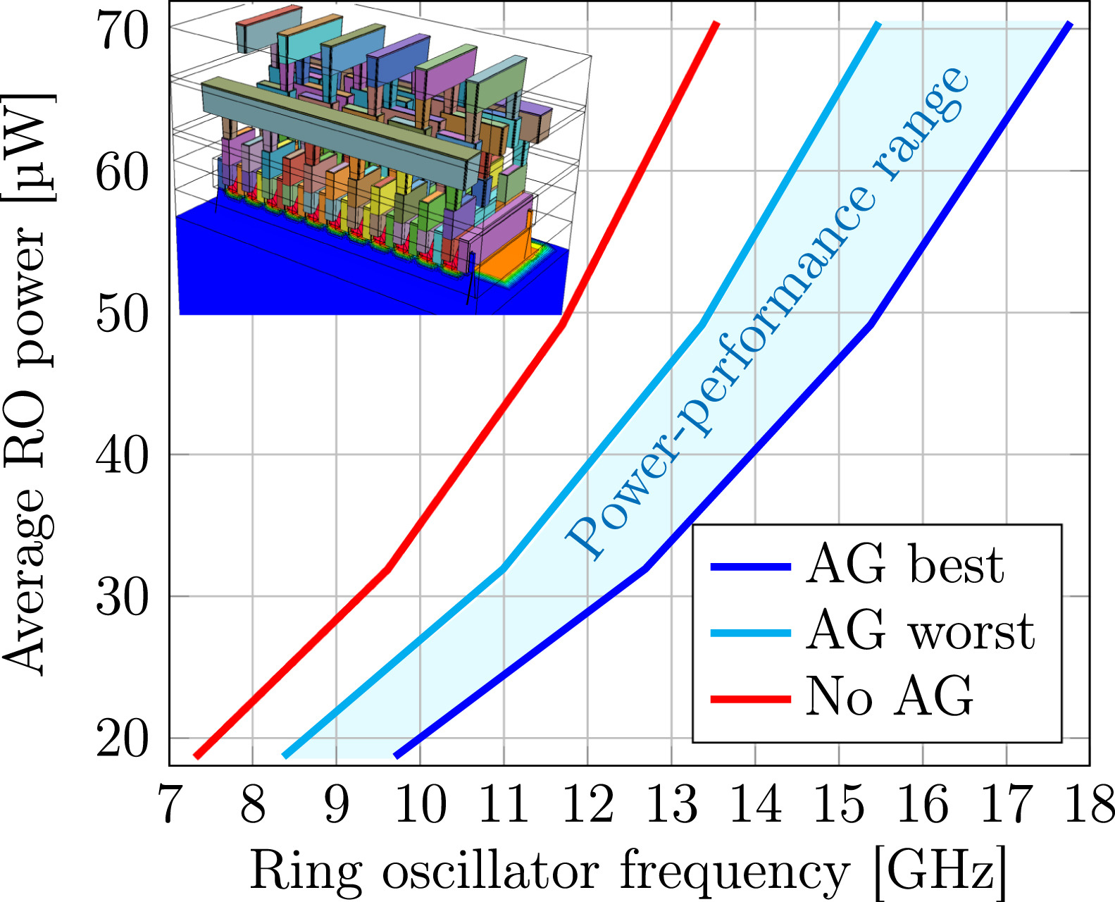
This flow was applied on two proposed fabrication flows, corresponding to cases when the air gap is created before and after the deposition of the first metal contacts layer. We have observed that introducing the air gap inside the spacer results in an at-least 15% improvement in the ring oscillator’s performance, when the power is kept constant. Further improvements can be achieved by reducing the conformal layer thickness and increasing the sticking probability by increasing the chamber partial pressure or reducing the temperature. The achieved power-performance range for the 5-stage ring oscillator is provided in Fig. 2.

Fig. 1: Flowchart showing the presented DTCO workflow (solid arrow) for air spacer generation for a 5-stage inverter ring oscillator logic cell. The dotted arrow shows the development of the analytical model, which is based on a calibrated physical model. The main input parameters are the sticking probability s and conformal SiN layer thickness tc, which are used to generate the air spacer geometry GAS. The impact of the studied fabrication parameters (s, tc) on the circuit power and performance are provided using a power-performance analysis (PPA) chart.

Fig. 2: Achieved power and performance for the ring oscillator with no air gap (AG) and with an AG under best and worst tested process conditions. The case with no air gap corresponds to a completely filled SiN spacer, while the inset shows the full ring oscillator cell.


