 |
|
||||
BiographyTomáš was born in Opava, Czech Republic, in 1992. He received his Bachelor degree in Mechatronics from Brno University of Technology in 2015. After an exchange year at the Norwegian University of Science and Technology, Norway, he enrolled in a Master program therein, receiving his Master's degree (MSc) in Physics in November 2018. In addition to his expertise in condensed-matter physics, Tomáš has previous experience working in the fields of numerical acoustics and robotics. Tomáš joined the Institute for Microelectronics am in July 2020, where he is working towards his doctoral degree in micromagnetic simulations for non-volatile magnetic memory devices. |
|||||
Multi-Physics Modeling of SOT-MRAM – Investigation of Thermal Effects
The ongoing scaling of microelectronic devices and circuit has started to reach its physical limit. The leakage current is rapidly increasing, while the transistor size and the conductor spacing decrease, resulting in an increase static power consumption of integrated circuits. A promising solution to mitigate this increase in power consumption is a shift to non-volatile memory technology, with the magnetoresistive random access memory (MRAM) being the most promising candidate to date. The two-terminal spin-transfer torque (STT)-MRAM has already become commercially available; however, its broader applicability is heavily limited due to its relatively slow writing speed (~10ns). The newer spin-orbit torque (SOT)-MRAM strongly lessens the problem by introducing an additional heavy metal layer (HM) below the free magnetic layer (FL). In the first initial switching phase, current passes throughout the HM which, due to a spin Hall effect, exerts a torque on the FL. To complete the switching, another mechanism needs to be applied, such as an external/internal magnetic field, two-pulse switching, or the STT.
During switching, strong currents heat up the MRAM cell, which leads to significant material parameter changes. To fully understand the switching processes, we couple charge, spin, magnetization, and temperature dynamics in our model, while investigating the effects of the increased temperature.
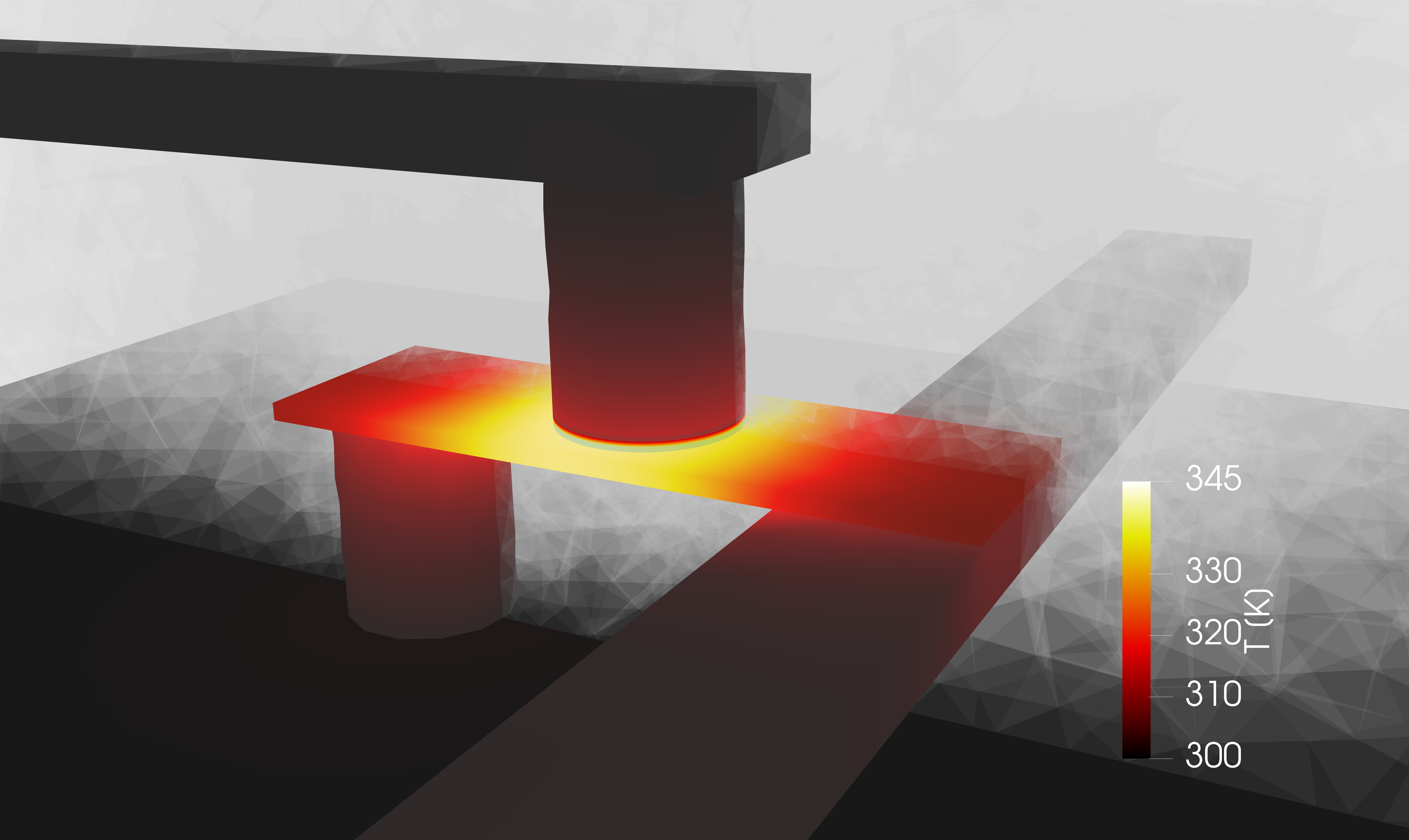
Fig. 1 shows a temperature simulation of a realistic SOT-MRAM cell with a magnetic tunnel junction (MTJ) diameter of 40 nm. On the left side, the heavy metal layer beneath the MTJ is contacted to a doped Si substrate to simulate a transistor structure, whereas the other side is contacted to a long metal interconnect. The top contact is likewise connected to a long metal interconnect. The entire structure is surrounded by an oxide layer to stabilize it. When a voltage pulse is applied between the sides of the HM, the temperature of the SOT-MRAM cells increases. The temperature increase is highest near the FL, which is clearly visible from Fig. 1.
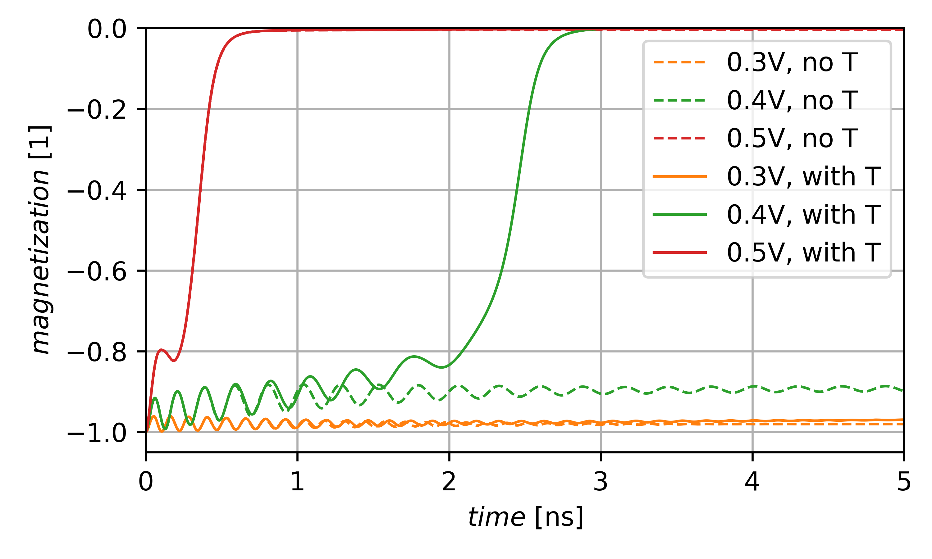
In Fig. 2, the effect of a slowly increasing temperature is provided. When no temperature parameter rescaling is used, the SOT is not strong enough to switch the FL magnetization in plane, when 0.4V is applied. In contrast, if a full simulation which includes temperature is carried out, the FL magnetization is eventually brought in plane. This long incubation time can be contributed to the slow temperature increase of the structure. As a result of the increased temperature, the critical switching current is reduced.

Fig. 1: Temperature of a realistic SOT-MRAM cell. When an electric field is applied across the HM, the passing currents cause the structure to heat up. The temperature is highest near the FL.

Fig. 2: Comparison between simulations with (dashed) and without (solid) temperature modeling. Due to the slowly increasing temperature, material parameters are changed, and the critical switching current is reduced.


