 |
|
||||
BiographyRoberto Lacerda de Orio studied electrical engineering at the University of Campinas (UNICAMP), Brazil, where he received his Bachelor degree in 2005 and his Master degree with emphasis on Microelectronics in 2006. He joined the Institute for Microelectronics in October 2006, where he received his doctoral degree in 2010 and worked as a post-doctoral researcher until 2013, with a focus on reliability issues in interconnects of integrated circuits. From 2014 to 2018 he was a tenured Assistant Professor at the Faculty of Electrical and Computer Engineering (FEEC) of UNICAMP, where he carried out research, teaching, and supervision activities of students at all academic levels in the area of micro- and nanoelectronics, mainly on topics related to the reliability of integrated circuits as well as the modeling, simulation, and fabrication of semiconductor devices. He was a Principal Investigator in research funded projects and also acted as Deputy Head of the Department of Semiconductors, Instruments and Photonics at FEEC/UNICAMP. In October 2018 he rejoined the Institute for Microelectronics as a research scientist (Postdoc) working on non-volatile magnetoresistive memory devices and supporting teaching activities. He has many years of experience in developing numerical simulation tools for micro- and nanoelectronic devices with programming skills in Python, C, and C++. Roberto is currently a Senior Scientist and is supporting the research related to robustness of electronic circuits, with a focus on the analysis of semiconductor physical phenomena and their reliability. He is also involved in lecturing for the Bachelor and Master programs at the Institute for Microelectronics, which includes programming in C, microelectronic devices simulation, modeling of electronic devices, and simulation of semiconductor devices fabrication. |
|||||
Impact of Voltage-Controlled Magnetic Anisotropy on Spin-Orbit Torque MRAM Switching
Magnetoresistive random access memory (MRAM) is currently an alternative technology employed as flash replacement in embedded systems. Its widest implementation is the well-matured spin-transfer torque (STT) MRAM. In order to concomitantly improve speed and reliability, MRAM cells based on spin-orbit torque (SOT) switching have been intensively investigated. SOT-MRAM can deliver ultrafast operation with sub-nanosecond timings, making it particularly suitable for cache memories, in replacement of conventional CMOS-based SRAM. Among the several field-free schemes which have been proposed, a promising candidate for future SOT-MRAM implementation is based on purely electrical control of the magnetization switching through the interplay of different physical mechanisms such as SOT, STT, and voltage control of magnetic anisotropy (VCMA). Recently, experimental results have indicated that such a scheme has the potential to achieve high-speed and low-power switching, while at the same time allowing for high-density integration.
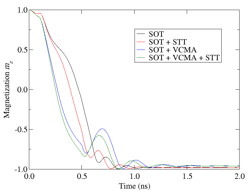
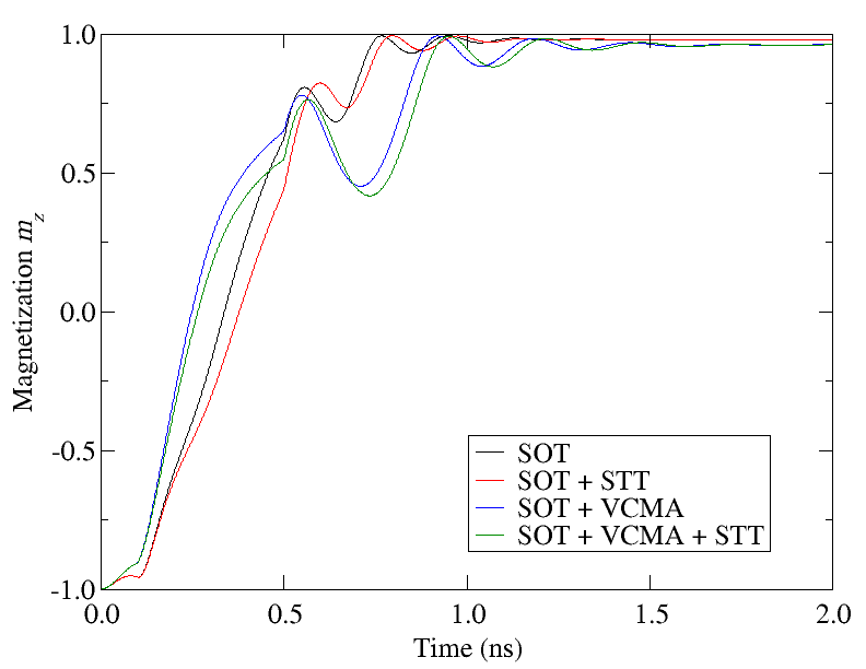
We have investigated how these different mechanisms, namely VCMA and STT, contribute to cell switching, when combined with SOT. Fig. 1 shows the z-component of the magnetization vector as a function of time for parallel to anti-parallel (P-AP) switching, while Fig. 2 presents the result for an anti-parallel to parallel (AP-P) transition, depending on whether VCMA and STT are considered or not. In both cases it can be verified that the magnetization reversal becomes faster, when the VCMA effect is active. In this case, an adequate voltage is applied across the MRAM cell, which reduces the magnetic anisotropy and, consequently, leads to a reduction in the energy barrier for the magnetization switching.
In turn, the effect of STT is less pronounced, but it influences the switching in opposite ways, depending on the transition direction. For a positive voltage applied across the device, the current flowing through the cell favors the AP state. Therefore, the resulting STT supports the P-AP switching and slightly accelerates it, as shown in Fig. 1. On the other hand, the STT tends to hinder the AP-P transition, slightly slowing it down, as shown in Fig. 2. Nevertheless, the VCMA effect has a more significant impact on the overall switching, in such a way that it facilitates the switching in both directions.

Fig. 1: Magnetization reversal, corresponding to P-AP switching, as a function of time, depending on the interplay of SOT, STT, and VCMA.

Fig. 2: Magnetization reversal, corresponding to AP-P switching, as a function of time, depending on the interplay of SOT, STT, and VCMA.


