 |
|
||||
BiographyViktor Sverdlov received his Master of Science and PhD degrees in physics from the State University of St.Petersburg, Russia, in 1985 and 1989, respectively. From 1989 to 1999 he worked as a staff research scientist at the V.A.Fock Institute of Physics, St.Petersburg State University. During this time, he visited ICTP (Italy, 1993), the University of Geneva (Switzerland, 1993-1994), the University of Oulu (Finland,1995), the Helsinki University of Technology (Finland, 1996, 1998), the Free University of Berlin (Germany, 1997), and NORDITA (Denmark, 1998). In 1999, he became a staff research scientist at the State University of New York at Stony Brook. He joined the Institute for Microelectronics, Technische Universität Wien, in 2004 and he is currently on a tenure-track position. His scientific interests include device simulations, computational physics, solid-state physics, and nanoelectronics. |
|||||
Edge Modes Conductance in Narrow MoS2 Nanoribbons in a Topological Phase
Novel monolayer-thin two-dimensional (2D) materials are promising candidates for advanced electronic device applications. 2D materials can typically also exist in several crystallographic phases. It has been theorized that the 1T’ MoS2 phase possess unique properties. The spin-orbit interaction opens a band gap of about 100 meV close to the intersection of the valence and the conduction bands. Since the top of the valence band lies above the bottom of the conduction band, the band structure is inverted, and the existence of peculiar edge states within the band gap is expected. In large samples the edge states are characterized by a linear dispersion. There are two edge states at each edge, which propagate in opposite directions. The two edge states also possess opposite spins. Because of this spin-momentum locking, back-scattering on a non-magnetic edge potential perturbation is not permitted. As the edge states are topologically protected against backscattering, they can perfectly carry the charge and spin currents even at nonideal edges, typical in experimental observations. A phase transition from the topologically nontrivial to a trivial insulating phase suppresses the existence of the edge states and the current flow. The phase transition is mediated by an electric field which is applied in a direction normal to the 2D sheet. The band gap is thereby reduced and can be completely closed, when increasing the electric field. The band gap reopens again at even larger fields; however, the material becomes a trivial insulator without any states within the bandgap.
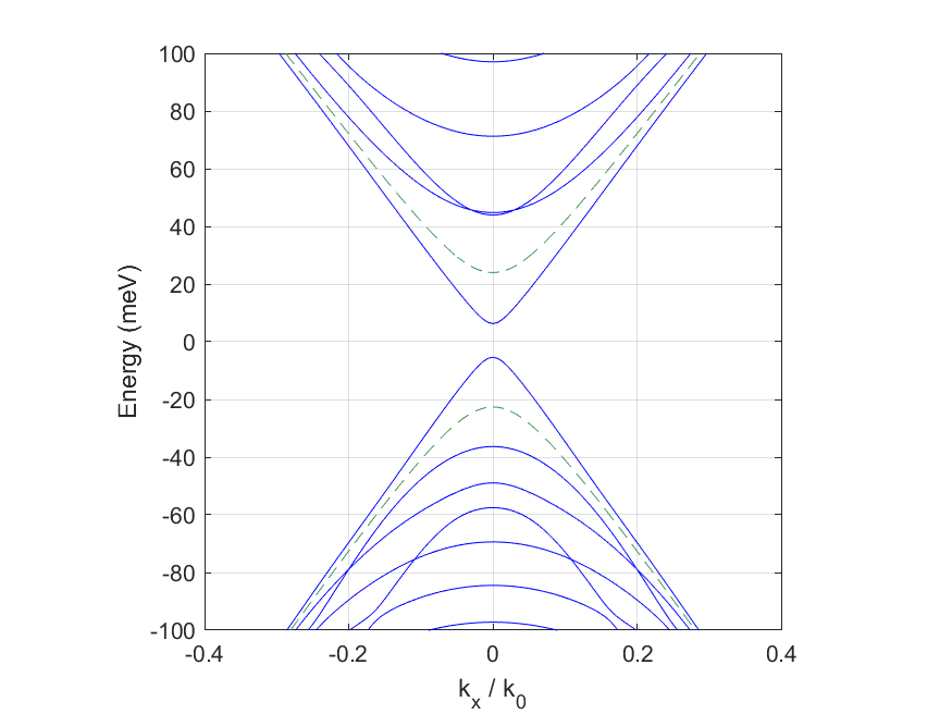
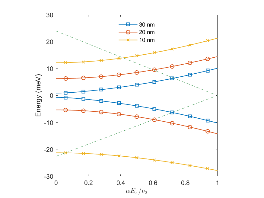
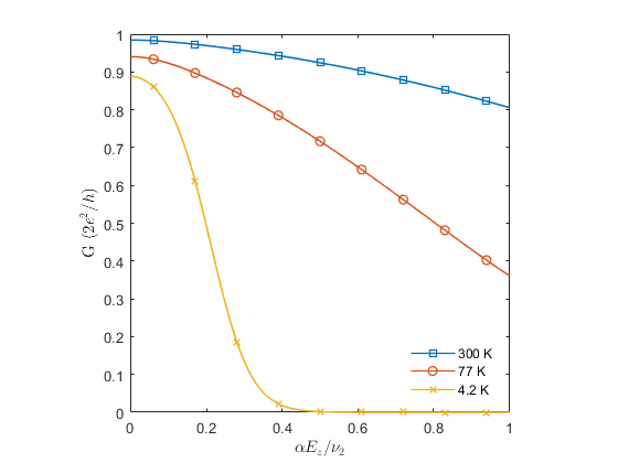
To increase the current, many edges with the current-carrying edge states are required. This can be realized by splitting a 2D sheet into many nanoribbons. In a MoS2 nanoribbon, however, the dispersion of the edge states becomes linear only at large momenta along the edges. At small momenta a tiny gap in the edge states spectrum opens, and their dispersion becomes quadratic (see Fig.1). The gap in the edge states dispersion increases with the increase of the normal electric field (see Fig.2). This results in a peculiar behavior of the ballistic conductance in a MoS2 nanoribbon with a width of 30 nm and Fermi energy EF=1.7 meV, as shown in Fig.3 at room, liquid nitrogen, and liquid helium temperatures.

Fig. 1: Subband structure in a MoS2 nanoribbon with a width of 20 nm. The subbands with a nearly linear dispersion and a tiny gap at small momenta correspond to the edge modes. Dashed lines: position of the extrema of the bulk dispersion.

Fig. 2: Subband gap dependence in a MoS2 nanoribbon with a width of 10 nm (stars), 20 nm (circles), and 30 nm (squares). The subband gap is larger in narrow nanoribbons and increases with the normal electric field. Dashed lines: the extrema of the bulk dispersion.

Fig. 3: Ballistic conductance as a function of the normal electric field in a MoS2 nanoribbon with a width of 30 nm for several temperatures: 300 K (squares), 77 K (circles), 4.2 K (crosses).


