 |
|
||||
BiographyKonstantinos was born in Vayia, Greece, in 1994. He received the Diploma of Electrical and Computer Engineering from the University of Patras in 2018. Between 2018 and 2020, he studied at the Physics department of the National Technical University of Athens, where he received the Master's degree in Microsystems and Nanodevices. In February 2020, Konstantinos joined the Institute for Microelectronics, where he is currently working towards his doctoral degree, focusing on the characterization and modeling of charge trapping in low-noise silicon transistors. |
|||||
Impact of Defects on the Threshold Voltage Drift in pMOS Transistors Employing SiO2
The time-dependent variability of metal-oxide-semiconductor field-effect transistors (MOSFETs) is heavily influenced by oxide and interface defects which can change their charge state through the capture or emission processes during operation. The charge capture and emission events have a significant impact on device electrostatics and may lead to drift in device characteristics. In modern nanoscale devices, the impact of a single defect is more pronounced than in large-area devices, resulting in charge emission events which are observable as discrete steps in the drain-source current during stress-recovery measurements. Furthermore, the fact that contributions from single defects increase in scaled nodes means that we can expect more significant variability between nominally identical devices, presenting considerable obstacles for developing robust electronic circuits. A statistical approach is required to evaluate charge-trapping effects at the single-defect level.
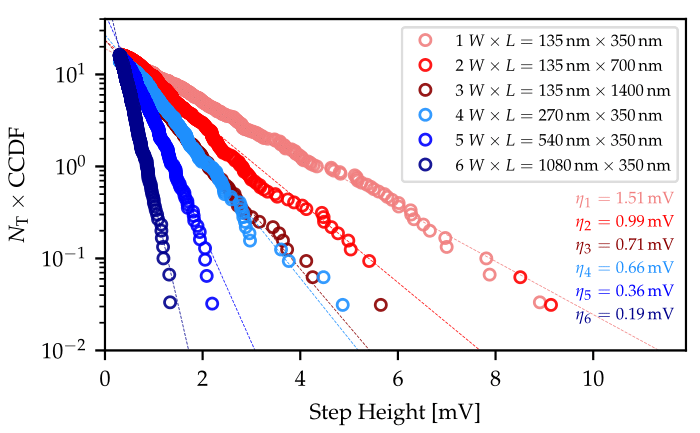
Creating and analyzing the complementary cumulative distribution function (CCDF) of step heights observed from stress-recovery measurements for each device type provides valuable insights into the average impact of defects on the device performance. To assess the experimental data, unimodal exponential distributions for the CCDFs for pMOS devices can be applied to enable the extraction of the average impact of a single charge transition (η) and the average number of defects per device (NT), as illustrated in Fig. 1.
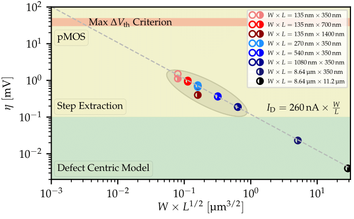
To enhance our understanding of how charge trapping affects device parameters, it is necessary to analyze data from a variety of devices with different gate areas, particularly those with equal gate areas but with varying widths (W) or lengths (L). Notably, devices with the same area, but different W/L ratios exhibit different η and NT values, suggesting that width and length impact η and NT differently. This observation challenges the widely recognized relation η∝1/(W×L) and implies that this relation may not be entirely accurate for the investigated technology and for operation close to the threshold voltage. As illustrated in Fig. 2, plotting η against W×√L captures all data points from experiments and the extracted values from the defect-centric model (DCM), demonstrating a stronger correlation with a trend towards W×√L than the typically assumed area scaling W×L. The less pronounced reliance on L might stem from the contrasting roles of length and width in percolative conduction.
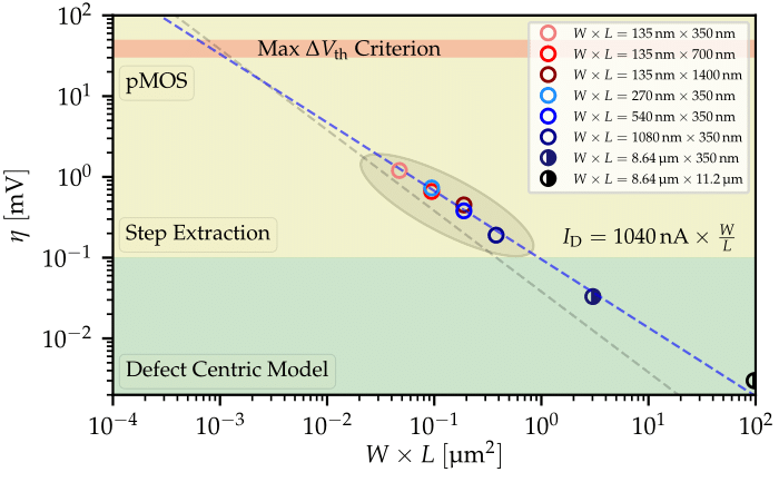
To evaluate the impact of the percolative conduction on the average step height, we measure a set of devices at recovery biases corresponding to operating conditions, where a more uniform means of conduction is anticipated due to the increased carrier density in the inversion layer. As depicted in Fig. 3, the η values from measurements near the on-state appear to follow the W×L area scaling. The values calculated from the DCM for the two large devices are also consistent. We anticipate that the η values will decrease, when measured at higher recovery biases due to the enhanced screening of trapped charges from the inversion layer. This observation highlights the relationship between the device geometry and the η values, providing further insight into the behavior of these devices under varying operating conditions and contributing to the ongoing efforts to optimize and enhance the performance of nanoscale transistors.

Fig. 1: The complementary cumulative distribution functions (CCDFs) for the step heights of hole traps, obtained following negative bias temperature instability (NBTI) stress testing on p-type metal-oxide-semiconductor (pMOS) devices are presented. The dashed lines illustrate the unimodal exponential distribution which has been employed as a suitable model to accurately represent and describe the observed experimental results from the stress tests.

Fig. 2: The η values are shown in relation to the W×√L trend, and the fitted line effectively encompasses both experimental data and values derived from the DCM model. In certain geometries, the markers representing experimental data (empty markers) and those from the DCM model (half-full markers) coincide. Their respective values are remarkably close, making it difficult to visualize any difference, when using a logarithmic scale.

Fig. 3: The η values corresponding to the on-state measurements are graphically represented against the W×L trend. The fitted line successfully encapsulates all data points gathered from various device geometries (empty markers) and the DCM values (half-full markers) specifically pertaining to the two larger geometries, providing a comprehensive understanding of the relationship between these parameters across diverse configurations.


