 |
|
||||
BiographyDominic Waldhör was born in Linz, Austria in 1992. He studied at the TU Wien, Vienna, Austria where he received the BSc degree in Electrical Engineering and the Diplomingenieur degree in Microelectronics and Photonics in 2018. He joined the Institute for Microelectronics in October 2018 where he works as PhD student. His current research focuses on the ab initio simulation of oxide defects in semiconductor devices. |
|||||
Silicon-Impurity Defects in Calcium Fluoride: A First Principles Study
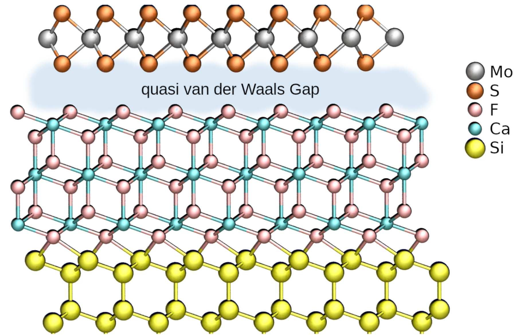
CaF2, or calcium fluoride, has demonstrated significant potential as a dielectric material in emerging two-dimensional (2D) electronic devices. Its wide bandgap of Eg=12.1 eV substantially reduces gate-leakage currents, when compared to other insulators commonly used for 2D devices, such as hexagonal boron nitride. Moreover, its chemically inert surface, resulting from the strong ionic bonding, allows for the formation of quasi-van der Waals interfaces with various 2D materials, including graphene and transition metal dichalcogenides (TMDs). A possible gate stack featuring CaF2 grown on an Si(111) substrate is illustrated in Fig. 1.
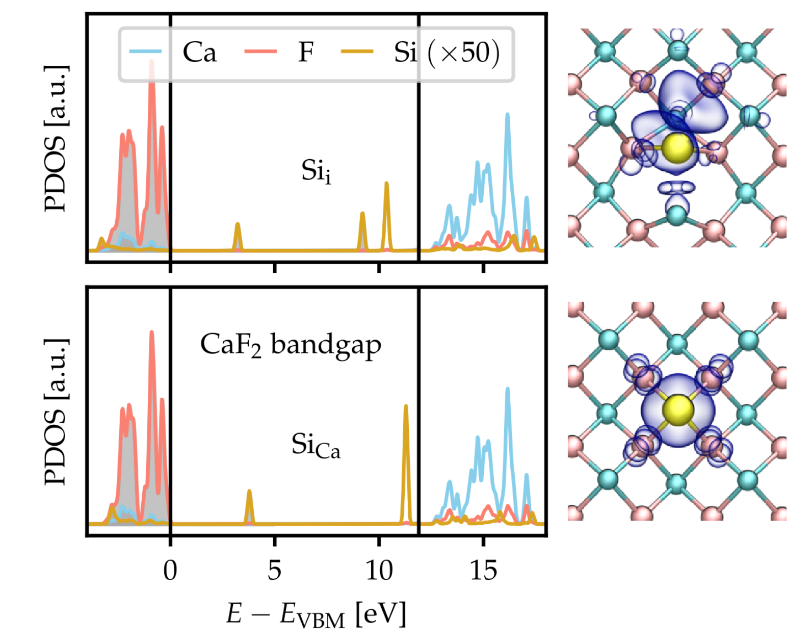
Despite its advantages as a gate dielectric, CaF2-based devices still exhibit greater hysteresis during gate voltage sweeps and a larger bias temperature instability (BTI) compared to established silicon technologies, currently employed in the semiconductor industry. Both of these phenomena are generally caused by charge trapping at defect sites in the insulator. In this work, we conduct a theoretical study based on density functional theory (DFT) to identify the possible defects which are responsible for BTI and hysteresis in CaF2-based devices. Specifically, we focus on silicon-impurity defects, as CaF2 is typically grown on a Si(111) substrate by molecular beam epitaxy (MBE) for device applications. During this process, individual Si atoms from the initial Si surface can be incorporated into the CaF2 film at interstitial sites (Sii) or replace a calcium atom (SiCa), as depicted in Fig. 2.
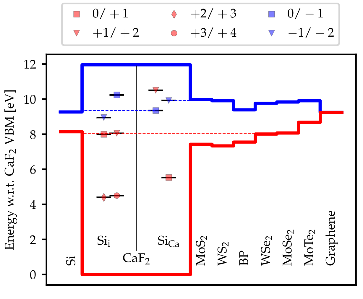
Utilizing DFT, we calculated the relaxation energy and the thermodynamic trap levels – the most crucial parameters governing charge trapping dynamics – for the Sii and SiCa defects. We discovered that both defects can exist in multiple charge states, ranging from -2 to +4, with trap levels across the CaF2 bandgap. As illustrated in Fig. 3, depending on the 2D semiconductor used, these trap levels can be energetically close to either the valence or conduction band, and thus can potentially act as electrically active charge trapping centers. Since the investigated defects are intrinsic to CaF2 grown on Si(111), they may be the limiting factor for device reliability in this material system.

Fig. 1: Si(111)/CaF2/MoS2 gate stack. Due to its good lattice match, CaF2 can be grown on Si(111) in thin layers. It provides a virtually defect-free quasi van der Waals interface to the 2D material and hence greatly improves the reliability of 2D devices.

Fig. 2: Projected density of states (PDOS) and localized highest occupied molecular orbitals of the Sii (top) and SiCa (bottom) defect. Both defects introduce localized states in the bandgap, as can be seen from the DOS projected onto the Si impurity. Note that the Si PDOS is scaled by a factor of 50 for illustration purposes.

Fig. 3: Trap levels of the Sii and SiCa defects within the bandgap of CaF2, together with the band edges of silicon and several commonly used 2D semiconductors. Alignments between band edges and active defect states are indicated with a dashed line.


