 |
|
||||
BiographyMichael Waltl is an Associate Professor of Robust Microelectronics, an IEEE Senior Member, and the director of the device characterization laboratory at the Institute for Microelectronics. He obtained his doctoral degree in technical sciences (summa cum laude) from TU Wien in 2016. Furthermore, he currently leads the Christian Doppler Laboratory for Single-Defect Spectroscopy and several FFG projects. In addition, Dr. Waltl heads several research projects with international industrial partners imec, ams OSRAM AG, Infineon, and more. In 2018 Dr. Waltl was a visiting researcher at imec, Belgium, Europe, and Stanford University, CA, USA. ). He also received a best paper award at IRPS 2014, a best poster award at the ICPTDC 2019, and co-recipient of the best student paper awards at the IIRW 2019, IEDM 2019, and DRC 2020. Dr. Waltl serves in the management committee of the IIRW, is a member of the technical program committee of various conferences in Europe (ESREF and the ESSDERC/ESSCIRC) and in the USA (IRPS and IEDM). He is an Associate Editor in the Microelectronics Engineering Journal and is a reviewer of numerous renowned Journals including Nature Electronics, IEEE TED, Microelectronics Reliability, Journal of Applied Physics, and many more. Research Interests:Michael Waltl’s overall scientific focus is on the robustness of microelectronic devices and circuits. In this field, he investigates reliability issues – characterization and modeling – in semiconductor devices and circuits. His research covers evaluating performance limitations and aging issues in silicon devices, devices employing wideband-gap materials, power electronic systems, and transistors built on novel 2D materials. Dr.Waltl also studies hot carrier degradation and stress-induced leakage currents of various transistor technologies. Another research pillar of Dr. Waltl is the high-performant operation of integrated circuits built from scaled devices, where he investigates the impact of defects on the performance of circuits. Also, his research focus is on radiation hardening of various technologies, i.e. SRAM cells, and integrated electronic circuits. Furthermore, Dr. Waltl has a strong background in measurement technology and is leading the development of novel characterization tools and techniques. Research Topics:Robust Electronic Circuits Projects:CDG - Christian Doppler Laboratory for Single-Defect Spectroscopy in Semiconductor Devices |
|||||
Challenges for Electronic Circuits Made from Devices Based on 2D Materials
In the last decade, 2D materials received significant attention in the search for novel materials in transistor technologies. The main advantage of 2D materials, compared to silicon, is the possibility of fabricating devices with channel thicknesses below 1 nm, which suppress short channel effects. Thus, field-effect transistors (FETs) fabricated using 2D semiconductors as their channel layer are expected to exhibit large carrier mobilities, nearly ideal sub-threshold slopes, and high on/off current ratios, opening the door towards ultra-scaled post-silicon technologies. While tremendous efforts have been invested into fabricating 2D transistor prototypes, while employing various material combinations, the research into 2D electronic applications is still in its infancy. So far, small digital circuits such as inverters, logic gates, ring oscillators (RO), static random access memory cells (SRAM), operational amplifiers, and a simple microprocessor have demonstrated stable operation, when designed using 2D materials-based FETs. The stable operation of the circuits strongly relies on the fabrication of transistors with well-defined properties, that is, process-controllable threshold voltage, large sub-threshold slope and on/off current ratio, but also small time-dependent parameter drifts to ensure a long lifetime. However, as evidenced by experimental studies, 2D transistors can still exhibit large variability, e.g., a threshold voltage variance of up to 1 V, which is a crucial issue for industrial applications.
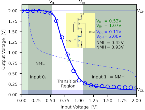
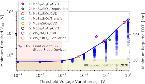
One of the basic logic circuits is the inverter. In CMOS technology, the inverter consists of a p-type FET connected in series with an n-type FET. For 2D technologies, the integration of n-type and p-type transistors has already been demonstrated by, for instance, using different channel materials. However, enabling the full scope of existing CMOS technologies for 2D technologies remains challenging. An alternative approach is the implementation of pseudo-CMOS (or nMOS) circuits, consisting only of n-type transistors. In the case of an inverter circuit, the static behavior can be described by its voltage transfer characteristics (VTC), shown in Fig. 1. From the VTC, the bias margins can be extracted, which describe the applied bias at which the inverter operates in a well-defined state. The higher the logic low noise margin (NML) and logic high noise margin (NMH) are, the more robust the inverter is against noise from other circuit elements or from external distortions, such as radiation. A change in the threshold voltage of one of the two transistors directly reduces NML and NMH. To ensure the proper operation of inverters based on equally balanced FETs, the maximum permitted variability for the threshold voltage is typically around 30 mV. A comparison with different 2D technologies shows that the WS2/HfO2 transistors are already very close to meeting targets for low voltage 2D inverters, see Fig. 2. In contrast, most published technologies require further optimization to comply with the IRDS targets for 2028.
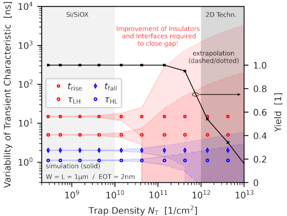
While the static VTC describes the bias levels under steady state conditions, the high-to-low and low-to-high transition times determine the dynamic behavior of inverter circuits. As seen in Fig. 3, the dynamic parameters can be heavily impacted by charge trapping, which increases the delay times during inverter operation. Furthermore, with increasing trap density, the obtained variability increases, resulting in jitter in the clock signals of digital circuits. In addition, large drifts of the threshold voltage can increase the device failure rate and thus decrease the yield, which is critical for defect densities above 1011cm-2. It should be noted that, for scaled devices, the variability increases and lower margins for defect densities are thus necessary for an acceptable yield. In summary, using 2D materials could help to overcome scaling and functional integration limitations from silicon technology, such as short channel effects and reduced charge carrier mobilities for extremely scaled devices, mainly because they can be fabricated as monoatomic sheets. At the current state-of-the-art, the operation of transistors and circuits designed using 2D materials has been demonstrated at the prototyping stage. However, the performance of 2D transistors suffers from defects at the channel/insulator interface and in the insulator, which can considerably degrade the characteristics of the devices and requires further optimization of device stability, before 2D circuits can become suitable for consumer electronics.

Fig. 1: The voltage transfer characteristic of an inverter circuit (inset) shows the bias levels which are interpreted as a logic low/high when VIL/VIH is applied at the input. The output voltages represent the logic low/high state VOL/VOH. In addition, the noise margin for logic low/high inputs NML/NMH is shown.

Fig. 2: Demands on 2D transistor technologies to enable circuits operating at conditions targeted by the IRDS specification for 2028. The graph illustrates how the variation of the threshold voltage of the two transistors comprising the inverter affects the minimum required VDD to achieve noise margins NML and NMH of at least 0.1×VDD.

Fig. 3: To evaluate the impact of trap distributions on the dynamic behavior of an inverter, we inspect the rise and fall time for a 2D pseudo-CMOS (nMOS) inverter circuit. For a trap density exceeding 1011cm-2, a significant variation in the timing characteristics is observed. Note that an improvement by two orders of magnitude in the trap density is still required for this novel technology to be suitable for digital electronic applications.


