 |
|
||||
BiographyChristoph Wilhelmer was born 1993 in Lienz, Austria. He received his Bachelor degree in Technical Physics from TU Wien after doing an exchange semester at the University of Bath, UK in 2017. He received his Diplom-Ingenieur degree in Technical Physics from TU Wien in 2020 where he carried out his Master Thesis in the Quantum Materials group of the Institute of Solid State Physics. In March 2020 he joined the Institute for Microelectronics where he started his PhD, focusing on defect creation mechanisms in oxides used for semiconductor applications. |
|||||
Intrinsic Charge Trapping Sites in Amorphous Si3N4
Amorphous silicon nitrides are widely used as the storage layer of charge trap flash memory devices. This is primarily due to the inherently high defect density in these materials and the long storage times of localized charges (~10 years at 80°C). While the Si-dangling bond or K-center has been identified in the past as a possible charge trapping site for electrons, the complete charge storage mechanism, including hole trapping and intrinsic charge trapping sites, is not fully understood yet.
We conduct ab initio investigations in amorphous Si3N4 to investigate the localization of holes and electrons in this material. The amorphous model structures were created by simulating a melt-and-quench procedure with a molecular dynamics (MD) algorithm. Therefore, we developed a machine-learned force field to employ in our simulations, which was trained solely on the energies, atomic forces, and stress tensors of thousands of Si3N4 structures from density functional theory (DFT) calculations. The resulting structures were geometry-optimized with a range-separated variant of the PBE0 hybrid functional and show excellent agreement with experimental properties of Si3N4 thin films. Furthermore, the model structures have low densities of over- and undercoordinated atoms, which allows for the investigation of specific charge trapping processes.
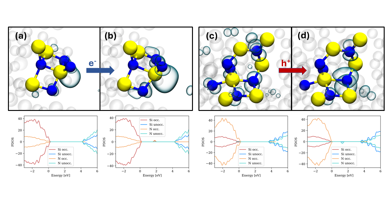
We find that overcoordinated nitrogen atoms introduce electronic states at the conduction band minimum (CBM). The corresponding lowest unoccupied molecular orbital (LUMO) is localized around a nearby Si atoms (dsee Fig. 1(a)). Additional electrons can get trapped at these sites, occupying this state, and moving it towards the middle of the band gap, as shown in Fig. 1(b). Similarly, the highest occupied molecular orbital (HOMO) is semi-localized at N atoms which are adjacent to overcoordinated Si, which correspond to a state at the valence band maximum (VBM), as shown in Fig. 1(c). An additional hole can get trapped at this site, which shifts the state at the VBM, now unoccupied, to the middle of the bandgap due to structural relaxations (see Fig. 1(d)). The thermodynamic charge transition levels of these states are close to the CBM and VBM for electron and hole traps, respectively, which shows that overcoordinated atoms are a possible source of intrinsic charge trapping centers, contributing to the storage mechanism in charge trap flash devices.

Fig. 1: Molecular orbitals localized near overcoordinated atoms with the corresponding projected density of states below. (a) LUMO localized at Si near four-fold coordinated N, no defect state in band gap; (b) additional electron localizes at this site and shifts the now occupied state near the middle of the band gap; (c) HOMO semi-localized at N near five-fold coordinated Si, no defect state in band gap; (d) additional hole localizes at one of the N atoms due to atomic relaxations and shifts the now unoccupied state near the middle of the bandgap.


