
 |
|
Biography
Lado Filipovic was born in Sarajevo, Yugoslavia in 1983. He studied electrical engineering at Carleton University, in Ottawa, Canada, where he received the degree of Bachelor in Electrical Engineering (2006) and Master in Applied Science (2009). He joined the Institute for Microelectronics in January 2010, where he completed his doctoral degree in December 2012. His scientific interest is focused on topography simulations of novel semiconductor processes and the effects of process variability on semiconductor geometries.
The Influence of Processing on the Performance and Reliability of Through Silicon Vias
Due to the anticipated limitations of device scaling with "more Moore" at the 6nm node and the increasing process and factory costs of scaling, a significant amount of effort has been directed towards "more than Moore" integration. This type of integration deals with the introduction of more functionality to applications beyond memory and logic. Three-dimensional integration, using a Through Silicon Via (TSV) process, is a promising technology which allows for the fabrication of systems connecting various technologies, dense device packing, lower power consumption, and reduced Resistive Capactive (RC) delay. A sequence of several sensitive processing steps are required in order to generate a TSV with a desired size and aspect ratio. In addition to the deposition of insulation and conducting materials, a method to etch vertical trenches through a silicon wafer is required. Modern efforts to etch highly vertical TSVs result in scalloped TSV sidewalls, which could affect TSV performance and reliability. Through simulations, the impact of processing on the electrical performance, stress response, and reliability of the TSV devices has been analyzed. A level set process simulator has been employed to generate structures under varying process conditions, resulting in varying scallop sizes along the etched sidewall. The deposition of oxide on these walls is also performed using well known Low-Pressure Chemical Vapour Deposition (LPCVD) models, resulting in the structures shown in Fig. 1.The presence of scallops has been shown to have a detrimental effect on the electrical performance of TSVs, with increasing parasitic capacitance, resistance, and high-frequency signal loss through the device. The presence of scallops introduced an increased TSV resistance, while increasing the scallop height resulted in further resistance increase. On a positive note, the presence of scallops along the sidewall allows for more movement under the influence of stress, resulting in a better stress response in the tungsten layer when compared to the flat TSV alternative, as shown in Fig. 2. However, the locations where two scallops meet is prone to very high stresses due to the pinch-off caused by the scallops' attempts to expand during a drastic change in temperature. Therefore, although the overall stress response through the tungsten is improved, some points of increased stress may still lead to failure. The electromigration-induced stress affects the bottom aluminum layer and not the sidewall tungsten itself; therefore, it is the thickness of this layer which determines the electromigration reliability of the TSV. Changing the shape, thickness, and scallop height of the tungsten itself is shown to not influence the electromigration response. It was noted that a thinner aluminum layer resulted in an increased current density, which directly increased the electromigration-induced stress.
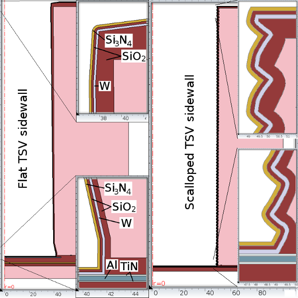
Fig. 1: Cross-sections of simulated TSV structures without (left) and with (right) the presence of scallops.
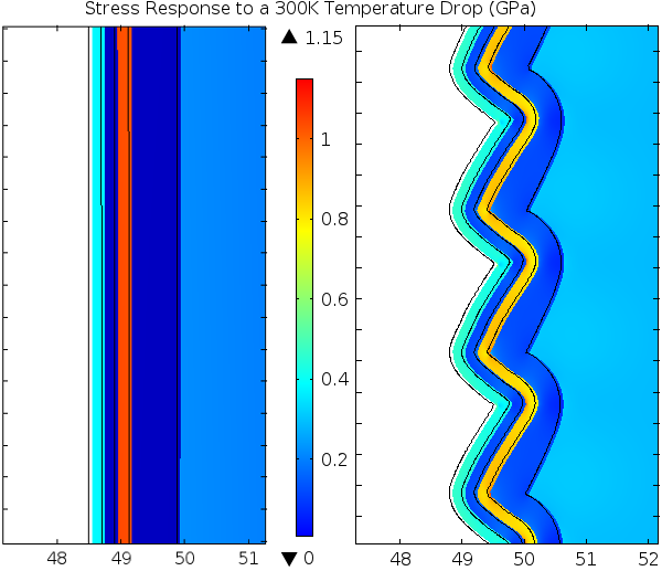
Fig. 2: Stress response to device cooling from 593K to 273K for scalloped and flat TSV structures.
