
 |
|
Biography
Lidija Filipovic was born in Sarajevo, Yugoslavia in 1982. She studied electrical engineering at Carleton University, in Ottawa, Canada, where she received the degree of Bachelor in Electrical Engineering in 2005 and Master of Applied Science in 2007. She joined the Institute for Microelectronics in March 2012, where she is currently working on her doctoral degree. Her scientific interest is focused on nanowire heterostructures and device simulation.
3D Modeling of Band-To-Band Tunneling
As Complementary Metal-Oxide-Semiconductor (CMOS) device miniaturization is reaching the limits of its potential, alternative devices are being studied in the search for a sufficient replacement. Tunneling devices have shown clear promise in providing a steep subthreshold swing, garnering much interest for ultra low power switching applications. The Band-To-Band (BTB) tunneling mechanism is complex and many factors affect the resulting current, making it a challenge to generate accurate models. Further complicating this system is the variation introduced by realistic 3D devices that is not accounted for in most commonly used 1D methods. An appropriate description of BTB tunneling in realistic devices necessitates a 3D approach.
We have developed a simple but effective model to describe direct BTB tunneling in 3D devices of arbitrary shape and varying effective mass. Our novel method re-formulates BTB tunneling into a single barrier problem. The computed single barrier exhibits valence band properties in some parts of the device, and conduction band properties in others. The location of these transitions are extracted by comparing the momenta of the two energy bands. Injected eigenmodes are calculated at contacts, and self-consistent wave functions are computed in the entire device. This computation is performed by solving the Quantum Transmitting Boundary Method (QTBM)-like Schrödinger equation.
This approach allows a study of the BTB tunneling barrier as it responds to changes in device geometry, material parameters and applied bias. By considering these parameters naturally, we are able to compute transmission coefficients and current for BTB tunneling in direct semiconductors with increased flexibility and improved accuracy.
The visualization of an effective BTB tunneling barrier location provides insight into wave propagation paths in real devices. Such 3D analysis of tunneling device configurations could be exploited to minimize the challenges faced by the novel devices and material combinations. Some possible applications are the study of tunneling barrier locations in gated devices, tapered NanoWire (NW) structures, doping profile variations, and various material combinations (direct-indirect junctions).
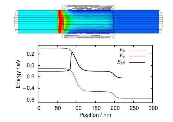
Fig. 1: BTB effective tunneling barrier for an InAs NW Tunneling Field-Effect Transistor (TFET).
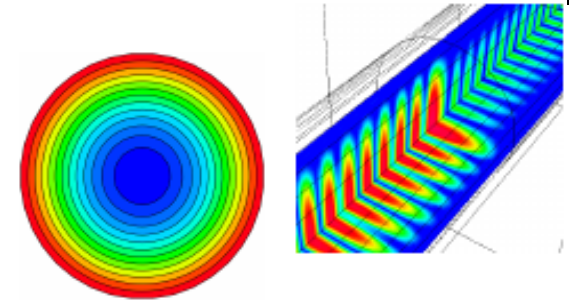
Fig. 2: Injected eigenmode and resulting propagating wave function through a p-n junction.
