
 |
|
Biography
Joydeep Ghosh was born in Kolkata, India. He studied electrical engineering (BSc) at the Jadavpur University, Kolkata. He was in IT industry for 3 years. Then he studied "Micro-nano science" (MSc) at the Technical University of Chemnitz, Germany, where he completed his studies in 2011. He joined the Institute for Microelectronics in March 2012. His current scientific interests include the drift diffusion equation with spin relaxation in silicon based semiconductor devices.
Influence of Charge Accumulation on Spin Transport in Silicon Based Devices
The scaling of Complementary Metal-Oxide-Semiconductor (CMOS) devices will reach fundamental limits in the near future, which necessitates the development of new technologies in the semiconductor industry. Spin-based electronics (spintronics) is a promising successor technology, which facilitates the spin as a degree of freedom. Silicon, due to its long spin lifetime and well established processes and technology, is an ideal material for spintronics. We investigate the electron spin and charge transport in an n-doped silicon bar with spin-dependent conductivity. The spin drift-diffusion model (coupled to the steady-state continuity equations and the Poisson equation) is considered, as it is widely used to describe the classical transport of charge carriers and their spins in a semiconductor. Our investigations can reproduce analytical solutions without the presence of a space-charge at the boundaries under an arbitrary external electric field. Injection (release) of charge causes a non-zero charge current in the device, and a significant spin and charge accumulation (depletion) can thereby also be introduced. In addition to the charge current, the spin current can diffuse out of this region. This spin current can be tuned by varying the applied voltage or changing the spin and the charge accumulation. We notice that the spin current in the bulk is reduced, when injected from a depletion layer, compared to an accumulation layer. This is caused by a lack of sufficient spin carriers. It is further noticed that injecting more charge at a boundary causes a screening effect, which only persists up to the classical charge Debye length. So, we observe that at a fixed interface spin polarization and when maintaining a fixed charge current, the interface spin current is enhanced through injecting more charge, but is almost unchanged in the bulk from that obtained at a Charge Neutrality (CN) condition (Fig. 1).Thus, injecting more spin and hence more charge does not result in a higher spin current in the bulk. As a result, at a fixed polarization, the CN condition determines the value of the possible maximum spin current, provided the charge current is the same.
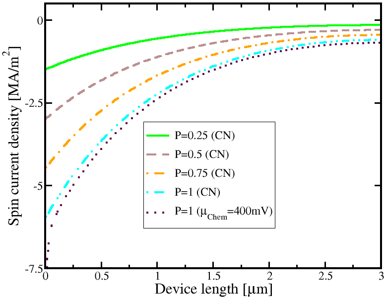
Fig. 1: Spin current density at different spin polarization (P), under CN condition. One plot is shown considering high charge accumulation. The charge current is zero.
