
 |
|
Biography
Wolfgang Gös was born in Vienna, Austria, in 1979. He studied technical physics at the Technische Universität Wien, where he received the degree of Diplomingenieur in 2005. In January 2006, he joined the Institute for Microelectronics and focussed on modeling of the bias temperature instability. In 2007, he was a visitor at the Vanderbilt University in Nashville, TN. In 2011, he received his doctoral degree and currently holds a post-doc position at the Institute for Microelectronics, where he continues his research activities in reliability issues of semiconductor devices. His current scientific interests include atomistic simulations, the chemical and physical processes involved in NBTI and HCI, and reliability issues in general.
Analogies of Charge Trapping in p- and n-Channel MOSFETs
The semiconductor industry has been struggling with reliability issues for years, in particular with Bias Temperature Instability (BTI). As the BTI degradation is most pronounced in p-channel Metal-Oxide-Semiconductor (pMOS) transistors, research has mainly focused on that defect and less attention has been paid to their n-channel MOS (nMOS) counterparts. But in the last years, increasing interest has emerged in understanding the degradation mechanisms in nMOS devices. Therefore, we have made intensive efforts to investigate positive BTI in nMOS experimentally. These studies were based on the Time-Dependent Defect Spectroscapy (TDDS) technique, which faces many experimental challenges, such as the resolution limit in the drain current. A series of defects in nMOS devices have been characterized, where some of them show a gate bias dependent emission behavior while others do not. A similar observation had already been made for traps in pMOS devices, where charge trapping is described by our four-state Non-radiative MultiPhonon (NMP) model. This has raised the question of whether charge trapping in both kinds of devices can be traced back to the same physical mechanism. Therefore, the four-state NMP model was adapted to the case of electron trapping, where the trapping dynamics still involve metastable states (1', 2') and as a consequence are based on the combination of the NMP and pure thermal transitions. From an atomistic perspective, the most noteworthy change in the model concerns the fact that now the capture of an electron, i.e., a negative charge, leads to structural relaxation. Using the modified four-state NMP model, good agreement with the experimental TDDS data could be achieved for both defects, with and without the bias dependent and independent emission times (confer Fig. 1 and Fig. 2). This suggests that charge trapping in pMOS and nMOS transistors follows the same physical mechanisms. As such, their different emission behavior could be ascribed to the discrepancy of switching and fixed oxide traps, as in the case of the pMOS analogon.
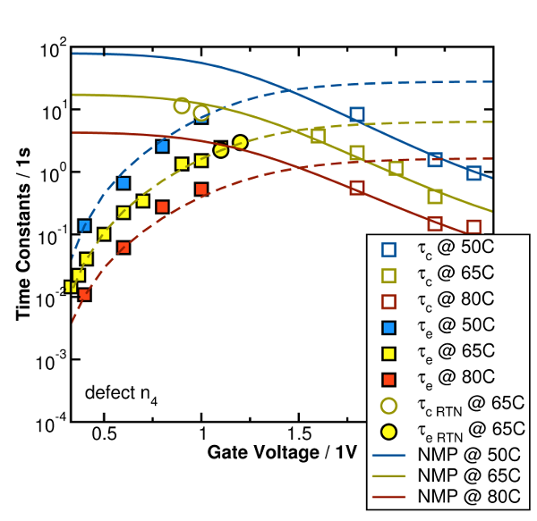
Fig. 1: Capture and emission time of defect #1. Similar to a fixed oxide hole trap, the emission time remains constant over the measured voltage range.
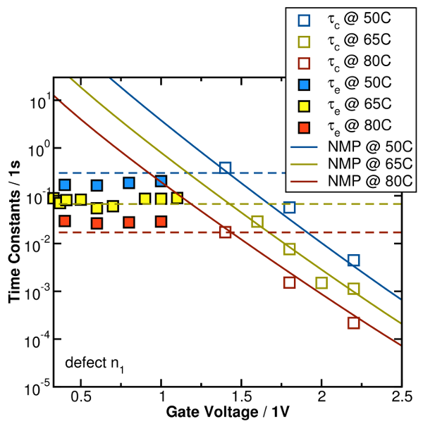
Fig. 2: Capture and emission time of defect #4. Its behavior resembles that of a switching-oxide hole trap with a bias sensitive emission time.
