
 |
|
Biography
Alexander Grill studied Microelectronics at the Technische Universität Wien, where he recieved his Diplomingenieur degree in 2013. Since March 2013 he is working on his doctoral degree at the Institute for Microelectronics. His scientific interests are the simulation of Nitride based heterostructure devices.
Threshold Voltage Drift in Gallium Nitride Based MIS-HEMTs
III-V nitride based materials, especially Gallium Nitride (GaN)-based devices, have been found to be good candidates for high-power, high-frequency and high-temperature applications. The reason behind this is that the GaN material system has some major advantages when compared to other materials. The first advantage is the large bandgap, which allows the design of power devices with very high breakdown voltages. The second advantage is the ability to design heterostructures using aluminum or indium doped barrier layers. The large spontaneous and piezoelectric polarization values lead to very high sheet carrier densities at the heterointerfaces, which enables the design of High-Electron Mobility Transistors (HEMTs) with high-power, low on-state resistance and fast switching dynamics.
Despite those superior material properties, widespread applications of GaN based devices are currently limited to laser diodes and microwave power transistors based on Schottky gates. In contrast to Schottky gates, devices with a gate dielectric have lower parasitic gate leakage currents. Unfortunately, they still suffer from threshold voltage (Vth) instability under forward bias conditions.
Currently, a physics based simulation model for the GaN material system, including a time dependent trap model to be able to explain the observed Vth drift, is under development. Despite recent efforts to characterize the traps responsible for threshold voltage drift, their origin and their electrical and physical properties are still a matter of debate. Vth-drift measurements suggest very fast trapping dynamics with a broad range of capture and emission times, which points to different types of involved defects. Bulk-type traps in the barrier region may contribute to Vth-drift, as well as interface traps at the dielectric interface and oxide traps in the dielectric itself. Under moderate gate stress, the availability of electrons in the barrier region can also act as a limiting factor for Vth drift dynamics. The modeling of these two effects, the physical nature of the involved traps and the transport of electrons from the channel to the traps require detailed and accurate models to still be developed and validated. Fig. 1 shows the small signal Capacitance-Voltage (CV) curve of a typical device.
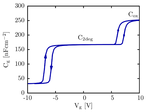
Fig. 1: Small signal CV behavior of a simple Metal-Insultator-Semiconductor HEMT structure. The amount of drift can be seen in the hysteresis of the two curves.
