
 |
|
Biography
Hans Kosina received the Diplomingenieur degree in electrical engineering and PhD from the Technische Universität Wien in 1987 and 1992, respectively. He was with the Institute of Flexible Automation at the Technische Universität Wien for one year and then joined the Institute for Microelectronics, where he is currently an associate professor. He received the venia docendi in microelectronics in 1998. In the summer of 1993, he was a visiting scientist at Motorola Inc., Austin, Texas, and in the summer of 1999, a visiting scientist at Intel Corp., Santa Clara, California. Dr. Kosina served as a Technical Program Committee member in the IEEE International Workshop on Computational Electronics in 2003 and 2004 and was the chairman of the ''11th International Workshop on Computational Electronics'' held in Vienna in May 2006. He has served as the Associate Editor of the IEEE Transactions on Computer-Aided Design of Circuits and Systems since January 2004. His current research interests include the device modeling of semiconductor devices, nanoelectronic devices, organic semiconductors and optoelectronic devices, the development of novel Monte Carlo algorithms for classical and quantum transport problems, and computer-aided engineering in ULSI-technology.
Thermoelectric Properties of Semiconductor Nanostructures and Nanostructured Tunnel FETs
A theoretical study of phonon transport in ultra-narrow Si nanowires has been peformed. An anomalous diameter dependence of thermal conductivity has been found (Fig. 1). The modified valence force field method in conjunction with coherent phonon transport has been employed. As the nanowre diameter is reduced from 12nm down to 1nn, the phonon density-of-states and transmission function acquire a finite value at low frequency, which is in contrast to bulk material where zero is approached. It turns out that this effect results in what Ziman described as the “problem of long longitudinal waves,” which states that the thermal conductivity of a material increases as its length is increased due to the vanishing scattering for long-wavelength phonons. We show that this thermal transport improvement also appears in nanowires as the diameter is decreased below 5 nm, originating from the increase in the density of the long wavevector modes. The effect is present under ballistic transport conditions, and further enhanced with the introduction of phonon-phonon scattering. In ultra-narrow nanowires, phonon transport is dominated more and more by lower energy phonons with longer mean-free paths as the diameter is reduced. We show that 80% of the heat is carried by phonons with energies less than 5meV, most with mean-free paths of several hundreds of nanometers.
Experimental evidence of a large thermoelectric power factor in heavily boron-doped p-type nanograined Si has been reported in literature. A power factor five times higher than in bulk Si has been observed. This enhancement occurs because for a specific range of carrier concentrations, both electrical conductivity and the Seebeck coefficient increase simultaneously. The two essential ingredients for this observation are nanocrystallinity and extremely high boron doping levels. We interpret this experimental finding using a theoretical model that considers both electron and phonon transport within the semiclassical Boltzmann approach. It is shown that transport takes place through two phases so that high conductivity is achieved in the grains, and high Seebeck coefficient by the grain boundaries. This together with the drastic reduction in the thermal conductivity due to boundary scattering could lead to a significant increase of the figure of merit ZT. This is one of the rare observations of a simultaneous increase in the electrical conductivity and Seebeck coefficient, resulting in enhanced thermoelectric power factor.
For the numerical study of tunnel Field-Effect Transistors (FETs), we have developed an effective model for direct band-to-band tunneling in 3D devices of arbitrary shape and varying effective mass. The method reformulates the interband tunneling problem into a single barrier problem. The computed single barrier exhibits valence band properties in some parts of the device, and conduction band properties in others. The location of these transitions are extracted by comparing the momenta of the two energy bands. Injected eigenmodes are calculated at contacts, and self-consistent wave functions are computed in the entire device. This computation is performed using the quantum transmitting boundary method.
The location of the effective tunneling barrier provides insight into the wave propagation path in real devices. Applications include the study of tunneling barrier locations in gated devices, tapered NW structures, doping profile variations, and the effect of various material combinations (direct-indirect junctions).
Recently, a graphene tunnel FET based on a vertical graphene heterostructure was proposed. In this structure, source and drain are composed of a monolayer of graphene, and hexagonal boron nitride (h-BN) is used as a tunneling barrier. The operation of this device is based on the voltage tunability of the density of states in graphene and on the effective height of the tunneling barrier. We have theoretically investigated device characteristics of vertical graphene tunnel FETs (Device 1) and graphene nanoribbon tunnel FETs (Device 2). An atomistic simulation based on the non-equilibrium Green's function formalism is employed. The results indicate that due to the presence of an energy gap in GNRs, Device 2 shows a much larger on/off-current ratio than Device 1. Furthermore, due to the smaller density of states and the resulting smaller quantum capacitance of GNRs as compared to graphene, better switching and frequency response can be achieved for Device 2.
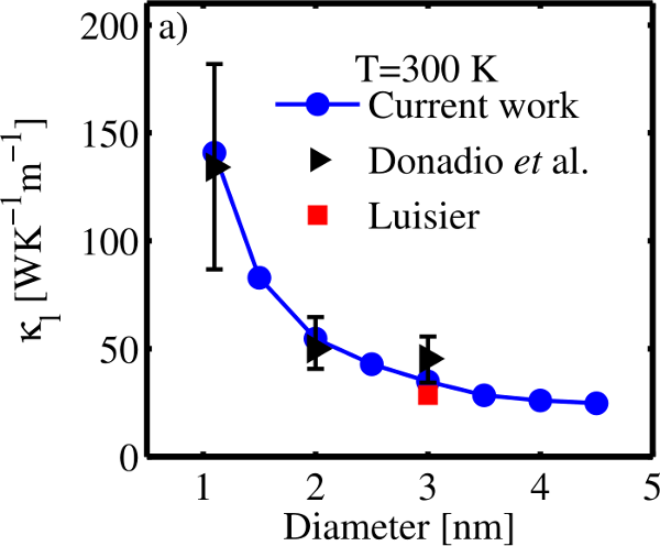
Fig. 1: Thermal conductivity of Si nanowires at room temperature limited by phonon-phonon scattering, as a function of diameter.
