
 |
|
Biography
Dmitry Osintsev was born in Volgograd, Russia in 1986. He studied computer science in Volgograd State Technical University, where he received the BSc degree in June 2007 and the MSc degree in June 2009. His current research interests are the ballistic regime of spin-polarized field-effect transistors.
Reduction of the Surface Roughness Induced Spin Relaxation in SOI Structures: An Analytical Approach
Spintronics presently attracts much interest because of the potential to build novel spin-based devices, which are superior to currently utilized charge-based electronics. Silicon is composed of nuclei with predominantly zero spin and it is characterized by small spin-orbit coupling. Both factors favour reducing spin relaxation. Understanding the details of the spin propagation in silicon structures is urgently needed.
We investigate the influence of the intrinsic spin-orbit interaction on the subband structure, spin scattering, and spin relaxation matrix elements due to surface roughness. The k·p Hamiltonian was obtained by changing the basis of the generalized Hamiltonian, which includes the spin degree of freedom. The Hamiltonian is written in the vicinity of the X point along the Z axis in the Brillouin zone. Four wave functions for the lowest spin up, spin down and for the second conduction band spin up, spin down are considered. The transformations are applied to get rid of the coupling between spins with opposite direction in different valleys. We then found wave functions in the same manner as for the two-band k·p Hamiltonian written in the vicinity of the X point of the Brillouin zone for silicon films under uniaxial strain.
The surface roughness scattering between the subbands is taken to be proportional to the square of the product of the subband wave function derivatives at the interface. Fig. 1 demonstrates an excellent agreement between the analytical solution and the numerically obtained results for a silicon film of 4nm thickness. For the numerical calculations, a barrier of 10eV height has been assumed. A strong decrease of the intersubband spin relaxation matrix elements when shear strain is increased is demonstrated in Fig. 2. The relaxation decreases for all three values of the film thickness. This decrease is a consequence of the fact that subband splitting increases with shear strain. As soon as intersubband splitting becomes larger than the spin-orbit interaction strength, the mixing of up- and down-spin states caused by this spin-orbit interaction is reduced.
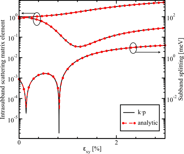
Fig. 1: Intrasubband scattering matrix elements normalized to their values at zero strain for the film thickness 1.36nm, and subband splitting as a function of shear strain.
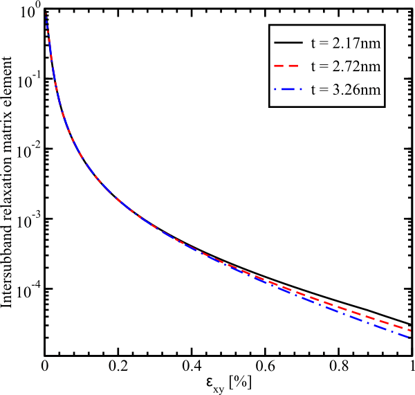
Normalized intersubband spin relaxation matrix elements as a function of shear strain for several values of the film thickness.
