
 |
|
Biography
Santo Papaleo was born in Novara, Italy, in 1988. He received the bachelor's degree in material science at the Università degli Studi del Piemonte-Orientale, and he received the master's degree in material science at the Università degli Studi di Milano-Bicocca in 2013. He joined the Institute for Microelectronics in 2013, where he is currently working on his doctoral degree. His scientific interests include stress estimation in TSV.
Stress Evolution During the Nanoindentation in TSV
Open Through Silicon Via (TSV) technology for 3D integration is considered necessary to maintain integrated circuit performance on the path described by Moore’s law. Several layers of different materials compose the TSV structure. It is important to understand and predict the behaviour of each material subjected to an external force. Although significant progress have been made in the mechanical characterization of the TSV structure, the stress development and the crack nucleation in each layer remains unclear. Nanoindentation enables us to study both the stress development in each layer of TSV, and the possibility of cracking and delamination. This technique is one of the most common experimental tools to test the mechanical properties of materials. Nanoindentation is based on an interaction between the tip and the material. The tip can have different shapes and it can be made of different materials. In our study we considered a diamond tip with different shapes. We use the Finite Element Method (FEM) to simulate and to understand stress development in the different layers composing the TSV. The tip penetrates into the device and applies force onto the material, causing the nanoindentation of the material. The comparison between the loading force and penetration depth allows for the obtaining of information about the mechanical properties of the device. The final goal is to understand how an external force influences the device structure and behaviour and if there is any development of defects during tip penetration, as the crack grows. Surface displacement profiles and stress fields are found to be sensitive to the thickness of the layers. A 2D axial-symmetric model was implemented in COMSOL-Multiphysics to simulate a general TSV structure. The results show the stress profile in the different layers with different materials and geometry. This FEM model will be applied to study the mechanical reliability of TSV.
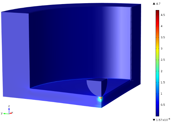
Fig. 1: Von Mises Stress at the bottom of the TSV during the nanoindentation.
